


TVS Diodes Datasheet
このカタログについて
| ドキュメント名 | Surface Mount SLD8S Series |
|---|---|
| ドキュメント種別 | 製品カタログ |
| ファイルサイズ | 726Kb |
| 取り扱い企業 | マウザー・エレクトロニクス (この企業の取り扱いカタログ一覧) |
この企業の関連カタログ


このカタログの内容
Page1
TVS Diodes Datasheet
SLD8S Series
Surface Mount
RoHS Pb e3
Description
The SLD8S Series TVS Diode is housed in a SMTO-263 package
with lead modifications. It is designed to protect sensitive
electronics against lightning and inductive load switching voltage
transient events for severe Automotive Load Dump applications.
Features & Benefits
■ AEC-Q101 qualified ■ Excellent clamping capability
■ S MTO-263 package, and foot ■ Low incremental surge
print is compatible to industrial resistance
popular DO-218AB package ■ UL Recognized compound
■ Meet ISO7637-2 5a/5b meeting flammability rating V-0
protection and ISO16750 load ■ Meets MSL level 1, per
dump test (refer to APP note J-STD-020, LF maximun peak
for details)
Agency Approvals of 260°C
■ VBR @ TJ= VBR@25°C x (1+αT ■ For surface mounted
x (T - 25))(αT:Temperature
Agency Agency File Number J applications to optimize board
Coefficient, typical value is space
E230531 0.1%
■ Low profile package
■ G lass passivated chip junction
in modified TO-263 package ■ High temperature to reflow
soldering guaranteed:
Maximum Ratings and Thermal Characteristics ■ ESD protection of data lines in 260°C/10sec at terminals
(T =25OC unless otherwise noted) accordance with IEC 61000-4-
A 2, 30kV(Air), 30kV(Contact) ■ Matte tin lead–free plated
■ EFT protection of data lines in ■ Halogen free and RoHS
Parameter Symbol Value Unit accordance with IEC 61000- compliant
Peak Pulse Power Dissipation 4-4 ■ Pb-free E3 means 2nd level
1. 10ms x 150ms test waveform 2200 W
■ F ast response time: typically interconnect is Pb-free and
PPPM
less than 1.0ps from 0 Volts to the terminal finish material is
2. 10/1000 test waveform 7000 W
BV min tin (Sn) (IPC/JEDEC J-STD-
Power dissipation on infinite heatsink at 609A.01)
TC = 25 °C PD 8.0 W
Maximum Instantaneous Forward Voltage
at 100A for Unidirectional only VF 1.8 V
Applications
Peak forward surge current 8.3m single
half sine-wave IFSM 1000 A
Designed to protect sensitive electronics from:
Operating Junction and Storage T , T -55 to 175 °C ■ Inductive Load Switching
Temperature Range J STG
■ Alternator Load Dump
Typical Thermal Resistance Junction to
case RƟJC 0.9 °C/W
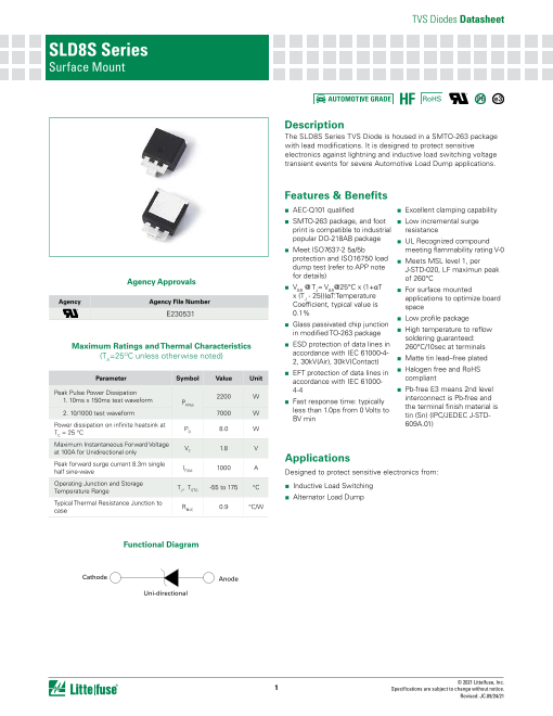
Functional Diagram
Bi-directional
Cathode Anode
Uni-directional
© 2021 Littelfuse, Inc.
1 Specifications are subject to change without notice.
Revised: JC.09/24/21
Page2
TVS Diodes Datasheet
SLD8S Series
Surface Mount
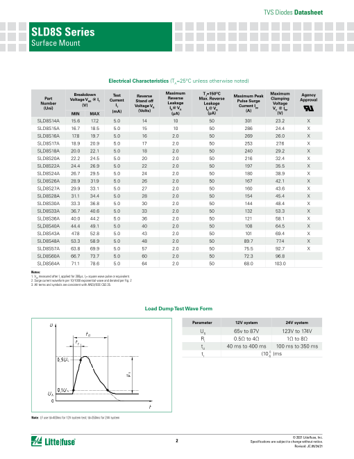
Electrical Characteristics (TA=25°C unless otherwise noted)
Breakdown Test Maximum TJ=150OC Maximum
Reverse Maximum Peak Agency
Part Voltage VBR @ IT Current Reverse Max. Reverse Clamping
Stand off Pulse Surge Approval
Number (V) I Leakage Leakage Voltage
T Voltage VR I @ V Current Ipp (Uni) I @ V V @ I
(mA) (Volts) R R R R (A) C PP
MIN MAX (µA) (µA) (V)
SLD8S14A 15.6 17.2 5.0 14 10 50 301 23.2 X
SLD8S15A 16.7 18.5 5.0 15 10 50 286 24.4 X
SLD8S16A 17.8 19.7 5.0 16 2.0 50 269 26.0 X
SLD8S17A 18.9 20.9 5.0 17 2.0 50 253 27.6 X
SLD8S18A 20.0 22.1 5.0 18 2.0 50 240 29.2 X
SLD8S20A 22.2 24.5 5.0 20 2.0 50 216 32.4 X
SLD8S22A 24.4 26.9 5.0 22 2.0 50 197 35.5 X
SLD8S24A 26.7 29.5 5.0 24 2.0 50 180 38.9 X
SLD8S26A 28.9 31.9 5.0 26 2.0 50 167 42.1 X
SLD8S27A 29.9 33.1 5.0 27 2.0 50 160 43.6 X
SLD8S28A 31.1 34.4 5.0 28 2.0 50 154 45.4 X
SLD8S30A 33.3 36.8 5.0 30 2.0 50 144 48.4 X
SLD8S33A 36.7 40.6 5.0 33 2.0 50 132 53.3 X
SLD8S36A 40.0 44.2 5.0 36 2.0 50 121 58.1 X
SLD8S40A 44.4 49.1 5.0 40 2.0 50 108 64.5 X
SLD8S43A 47.8 52.8 5.0 43 2.0 50 101 69.4 X
SLD8S48A 53.3 58.9 5.0 48 2.0 50 89.7 77.4 X
SLD8S57A 63.8 69.9 5.0 57 2.0 50 75.5 92.7 X
SLD8S60A 66.7 73.7 5.0 60 2.0 50 72.3 96.8
SLD8S64A 71.1 78.6 5.0 64 2.0 50 68.0 103.0
Notes:
1. VBR measured after IT applied for 300µs, IT= square wave pulse or equivalent.
2. Surge current waveform per 10/1000 exponential wave and derated per Fig. 2
3. All terms and symbols are consistent with ANSI/IEEE C62.35.
Load Dump Test Wave Form
Parameter 12V system 24V system
US 65v to 87V 123V to 174V
Ri 0.5Ω to 4Ω 1Ω to 8Ω
td 40 ms to 400 ms 100 ms to 350 ms
tr (10 0
-5 )ms
Note: LF use td=400ms for 12V system test; td=350ms for 24V system
© 2021 Littelfuse, Inc.
2 Specifications are subject to change without notice.
Revised: JC.09/24/21
Page3
TVS Diodes Datasheet
SLD8S Series
Surface Mount
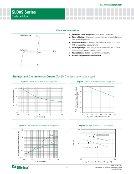
I-V Curve Characteristics
Uni-directional PPPM Peak Pulse Power Dissipation -- Max power dissipation
VR Stand-off Voltage -- Maximum voltage that can be applied to the
TVS without operation
VBR Breakdown Voltage -- Maximum voltage that flows though the
TVS at a specified test current (IT)
VC Clamping Voltage -- Peak voltage measured across the TVS at a
Vc VBR VR V specified Ippm (peak impulse current)
IR VF
IT IR Reverse Leakage Current -- Current measured at VR
VF Forward Voltage Drop for Uni-directional
Ipp
Ratings and Characteristic Curves (TA=25°C unless otherwise noted)
Figure 1 - Peak Pulse Power Rating Curve Figure 2 - Peak Pulse Power Derating Curve
100
100
80
10 60
40
1
20
0.1 0
0.01 0.1 1 10 100 0 25 50 75 100 125 150 175
td-Pulse Width (ms) TJ - Initial Junction Temperature (ºC)
Figure 3 - Typical Transient Thermal Impedance Figure 4 - Typical Junction Capacitance
100 100
R Uni-directional@V= 0V
θJA
10
R θJC
1 10
Uni-directional@ V= VR
0.1
0.01 1
0.01 0.1 1 10 100 10 100
t - Pulse Width (s) VBR - Reverse Breakdown Voltage (V)
© 2021 Littelfuse, Inc.
3 Specifications are subject to change without notice.
Revised: JC.09/24/21
PPPM-Peak Pulse Power(kW)
Transient Thermal Impedance (°C/W)
Cj (nF)
Peak Pulse Power (PPP) or Current (IPP)
Derating in Percentage %
Page4
TVS Diodes Datasheet
SLD8S Series
Surface Mount
Figure 5 - Typical SOA Chart
0.50 ISO7637 5A 12V Test System 0.50 ISO7637 5A 12V Test System
0.75 0.75
SLD8S14A SLD8S20A
SLD8S15A SLD8S24A
1.00 1.00
1.25 1.25
Td:400ms
Td:400ms
1.50 1.50
1.75 1.75
65 70 75 80 85 65 70 75 80 85
Vs(volt) Vs(volt)
1.5 ISO7637 5A 24V Test System
2.0
SLD8S30A
SLD8S36A
2.5
3.0
Td:350ms
3.5
4.0
123 133 143 153 163 173
Vs(volt)
Note: SOA (Safe Operation Area) refer to the area which below the curve line and refer to APP note for details.
Soldering Parameters
Reflow Condition Pb – Free assembly
- Temperature Min (Ts(min)) 150°C tP
Pre Heat - Temperature Max (T TP
s(max)) 200°C
- Time (min to max) (ts) 60 – 180 secs Ramp-up
Average ramp up rate (Liquidus Temp) (T ) to TL
L
peak 5°C/second max t
T L
S(max)
TS(max) to TL - Ramp-up Rate 5°C/second max Ramp-down
Preheat
- Temperature (TL) (Liquidus) 217°C
Reflow T
- Time ( min to max) (TS) 60 – 150 seconds S(min)
tS
Peak Temperature (T ) 260+0/-5
P °C
Time within 5°C of actual peak Temperature (tp) 20 – 40 seconds 25
time to peak temperature
Ramp-down Rate 5°C/second max Time
Time 25°C to peak Temperature (TP) 8 minutes Max.
Do not exceed 260°C
© 2021 Littelfuse, Inc.
4 Specifications are subject to change without notice.
Revised: JC.09/24/21
Ri(ohm) Ri(ohm)
Temperature
Ri(ohm)
Page5
TVS Diodes Datasheet
SLD8S Series
Surface Mount
Physical Specifications Environmental Specifications
Terminal Finish 100% Matte Tin-plated High Temp. Storage JESD22-A103
UL Recognized compound meeting HTRB JESD22-A108
Body Material
flammability rating V-0
Temperature Cycling JESD22-A104
Lead Material Copper Alloy MSL JEDEC-J-STD-020, LEVEL 1
H3TRB JESD22-A101
RSH JESD22-A111
Dimensions
F
B
G
Inches Millimeters
Dimensions
Min Max Min Max
H A 0.568 0.600 14.44 15.24
A
B 0.380 0.420 9.65 10.67
E C 0.098 0.114 2.50 2.90
D
J D 0.169 0.189 4.30 4.80
U E 0.102 0.118 2.60 3.00
C I
TOP VIEW SIDE VIEW F 0.178 0.188 4.52 4.78
G 0.045 0.060 1.14 1.52
AREA: 0.11 IN2 0.413
0.085 (10.50) H 0.360 0.370 9.14 9.40
(2.16)
I 0.106 0.122 2.69 3.09
0.331 J 0.069 0.089 1.75 2.25
0.276 (8.41) 0.276
(7.01) (7.01) M 0.284 0.300 7.22 7.62
0.601
(15.27) U 0 0.010 0 0.25
0.032 0.350
(0.81) (8.89)
0.091
(2.30)
M
0.320
(8.13) 0.118
(3.00)
BOTTOM VIEW RECOMMEND SOLDERING
PAD OUTLINE
Part Numbering System Part Marking System
SLD 8 S XX A
5% Voltage Tolerance
SLD8SXXX
Voltage YMXXX
SMTO-263 package
Power Dissipation
Series Code
© 2021 Littelfuse, Inc.
5 Specifications are subject to change without notice.
Revised: JC.09/24/21
Littelfuse Logo
Cathode Band
F
Y: Year Code
M: Month Code
XXX:Lot Code
Date Code Marking
Page6
TVS Diodes Datasheet
SLD8S Series
Surface Mount
Packaging
Part Number Component Package Quantity Packaging Option
SLD8SxxA SMTO-263 500 Embossed Carrier
SMTO-263 Embossed Carrier Reel Pack (RP) Specifications
Meets all EIA-481-2 Standards
0.63 0.157
(16.0) (4.0)
0.059 DIA
(1.5)
0.945 0.827
(24.0) *
(21.0)
* Cover tape
12.99
0.512 (13.0) Arbor (330.0)
Hole Dia. Dimensions
are in inches
(and millimeters).
1.01
(25.7)
Direction of Feed
Disclaimer Notice - Information furnished is believed to be accurate and reliable. However, users should independently evaluate the suitability of and test each product selected for their own applications. Littelfuse products are
not designed for, and may not be used in, all applications. Read complete Disclaimer Notice at http://www.littelfuse.com/disclaimer-electronics.
© 2021 Littelfuse, Inc.
6 Specifications are subject to change without notice.
Revised: JC.09/24/21