


AD5412/AD5422 Single Channel, 12-/16-Bit, Serial Input, Current
製品カタログ
Source and Voltage Output DACs, HART Connectivity
このカタログについて
| ドキュメント名 | AD5412/AD5422 Single Channel, 12-/16-Bit, Serial Input, Current |
|---|---|
| ドキュメント種別 | 製品カタログ |
| ファイルサイズ | 1.3Mb |
| 取り扱い企業 | マウザー・エレクトロニクス (この企業の取り扱いカタログ一覧) |
この企業の関連カタログ


製品カタログ
マウザー・エレクトロニクス

このカタログの内容
Page1
FEATURES、APPLICATIONS、GENERAL DESCRIPTION、COMPANION PRODUCTS
Single Channel, 12-/16-Bit, Serial Input, Current
Source and Voltage Output DACs, HART Connectivity
Data Sheet AD5412/AD5422
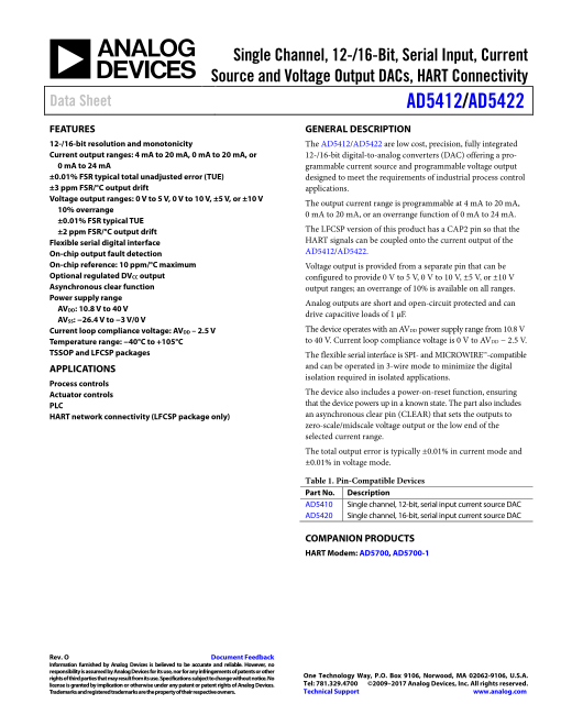
FEATURES GENERAL DESCRIPTION
12-/16-bit resolution and monotonicity The AD5412/AD5422 are low cost, precision, fully integrated
Current output ranges: 4 mA to 20 mA, 0 mA to 20 mA, or 12-/16-bit digital-to-analog converters (DAC) offering a pro-
0 mA to 24 mA grammable current source and programmable voltage output
±0.01% FSR typical total unadjusted error (TUE) designed to meet the requirements of industrial process control
±3 ppm FSR/°C output drift applications.
Voltage output ranges: 0 V to 5 V, 0 V to 10 V, ±5 V, or ±10 V The output current range is programmable at 4 mA to 20 mA,
10% overrange 0 mA to 20 mA, or an overrange function of 0 mA to 24 mA.
±0.01% FSR typical TUE
±2 ppm FSR/°C output drift The LFCSP version of this product has a CAP2 pin so that the
Flexible serial digital interface HART signals can be coupled onto the current output of the
On-chip output fault detection AD5412/AD5422.
On-chip reference: 10 ppm/°C maximum Voltage output is provided from a separate pin that can be
Optional regulated DVCC output configured to provide 0 V to 5 V, 0 V to 10 V, ±5 V, or ±10 V
Asynchronous clear function output ranges; an overrange of 10% is available on all ranges.
Power supply range Analog outputs are short and open-circuit protected and can
AVDD: 10.8 V to 40 V drive capacitive loads of 1 µF.
AVSS: −26.4 V to −3 V/0 V
Current loop compliance voltage: AVDD – 2.5 V The device operates with an AVDD power supply range from 10.8 V
Temperature range: −40°C to +105°C to 40 V. Current loop compliance voltage is 0 V to AVDD − 2.5 V.
TSSOP and LFCSP packages The flexible serial interface is SPI- and MICROWIRE™-compatible
APPLICATIONS and can be operated in 3-wire mode to minimize the digital
isolation required in isolated applications.
Process controls
Actuator controls The device also includes a power-on-reset function, ensuring
PLC that the device powers up in a known state. The part also includes
HART network connectivity (LFCSP package only) an asynchronous clear pin (CLEAR) that sets the outputs to
zero-scale/midscale voltage output or the low end of the
selected current range.
The total output error is typically ±0.01% in current mode and
±0.01% in voltage mode.
Table 1. Pin-Compatible Devices
Part No. Description
AD5410 Single channel, 12-bit, serial input current source DAC
AD5420 Single channel, 16-bit, serial input current source DAC
COMPANION PRODUCTS
HART Modem: AD5700, AD5700-1
Rev. O Document Feedback
Information furnished by Analog Devices is believed to be accurate and reliable. However, no
responsibility is assumed by Analog Devices for its use, nor for any infringements of patents or other
rights of third parties that may result from its use. Specifications subject to change without notice. No One Technology Way, P.O. Box 9106, Norwood, MA 02062-9106, U.S.A.
license is granted by implication or otherwise under any patent or patent rights of Analog Devices. Tel: 781.329.4700 ©2009–2017 Analog Devices, Inc. All rights reserved.
Trademarks and registered trademarks are the property of their respective owners. Technical Support www.analog.com
Page2
AD5412/AD5422 Data Sheet
TABLE OF CONTENTS
Features .............................................................................................. 1 Fault Alert .................................................................................... 35
Applications ....................................................................................... 1 Voltage Output Short Circuit Protection ................................ 35
General Description ......................................................................... 1 Voltage Output Overrange ........................................................ 35
Companion Products ....................................................................... 1 Voltage Output Force-Sense ..................................................... 35
Revision History ............................................................................... 3 Asynchronous Clear (CLEAR) ................................................. 35
Functional Block Diagram .............................................................. 4 Internal Reference ...................................................................... 35
Specifications ..................................................................................... 5 External Current Setting Resistor ............................................ 35
AC Performance Characteristics .............................................. 10 Digital Power Supply .................................................................. 36
Timing Characteristics .............................................................. 10 External Boost Function............................................................ 36
Absolute Maximum Ratings .......................................................... 13 External Compensation Capacitor........................................... 36
ESD Caution ................................................................................ 13 HART Communication ............................................................. 36
Pin Configurations and Function Descriptions ......................... 14 Digital Slew Rate Control .......................................................... 36
Typical Performance Characteristics ........................................... 16 IOUT Filtering Capacitors (LFCSP Package) ............................. 37
General ......................................................................................... 16 Applications Information .............................................................. 39
Voltage Output ............................................................................ 18 Voltage and Current Output Ranges on the Same Terminal 39
Current Output ........................................................................... 23 Driving Inductive Loads ............................................................ 39
Terminology .................................................................................... 27 Transient Voltage Protection .................................................... 39
Theory of Operation ...................................................................... 29 Galvanically Isolated Interface ................................................. 39
Architecture ................................................................................. 29 Microprocessor Interfacing ....................................................... 39
Serial Interface ............................................................................ 30 Layout Guidelines....................................................................... 40
Power-On State ........................................................................... 31 Thermal and Supply Considerations ....................................... 40
Data Register ............................................................................... 33 Industrial Analog Output Module ........................................... 41
Control Register .......................................................................... 33 Industrial HART Capable Analog Output Application ........ 41
Reset Register .............................................................................. 34 Outline Dimensions ....................................................................... 43
Status Register ............................................................................. 34 Ordering Guide .......................................................................... 44
AD5412/AD5422 Features ............................................................ 35
Rev. O | Page 2 of 44
Page3
REVISION HISTORY
Data Sheet AD5412/AD5422
REVISION HISTORY
10/2017—Rev. N to Rev. O Changes to Table 21 ........................................................................ 33
Changed CP-40-10 to CP-40-1 .................................... Throughout Changes to Thermal and Supply Considerations Section ......... 38
Updated Outline Dimensions ........................................................ 43 Changes to Table 25 ........................................................................ 39
Changes to Ordering Guide ........................................................... 44
7/2012—Rev. E to Rev. F
3/2017—Rev. M to Rev. N Updated Outline Dimensions........................................................ 40
Changed CP-40-9 to CP-40-10 .................................... Throughout Changes to Ordering Guide ........................................................... 40
Changes to Table 6 .......................................................................... 13
Changes to Figure 85 ...................................................................... 43 5/2012—Rev. D to Rev. E
Updated Outline Dimensions ........................................................ 43 Reorganized Layout ........................................................... Universal
Changes to Ordering Guide ........................................................... 44 Changes to Product Title.................................................................. 1
Changes to Features Section, Applications Section, and General
7/2016—Rev. L to Rev. M Description Section; Added Companion Products Section ............. 1
Changed −40°C to +85°C to −40°C to +105°C and CP-40-1 to Changes to Figure 1 .......................................................................... 3
CP-40-9 ........................................................................... Throughout Change to Offset Error Temperature Coefficient (TC)
Changes to Table 2 ............................................................................ 5 Parameter, Table 1 ............................................................................. 4
Added Table 3; Renumbered Sequentially ..................................... 9 Changes to Table 6 .......................................................................... 12
Changes to Figure 6......................................................................... 14 Changes to Power-On State Section ............................................. 29
Changes to Thermal and Supply Conditions Section ................ 40 Added HART Communication Section and Figure 68,
Updated Outline Dimensions ........................................................ 43 Renumbered Sequentially .............................................................. 33
Changes to Ordering Guide ........................................................... 44 Added Voltage and Current Output Ranges on the Same
Terminal Section and Figure 74 .................................................... 36
7/2015—Rev. K to Rev. L Added Industrial HART Capable Analog Output Application
Change to IOUT to GND Parameter, Table 5 ................................. 11 Section .............................................................................................. 38
Change to Voltage and Current Output Ranges on the Same Added Figure 79 .............................................................................. 39
Terminal Section ............................................................................. 37
11/2011—Rev. C to Rev. D
3/2015—Rev. J to Rev. K Changes to Table 15 ........................................................................ 29
Changes to Table 4 ............................................................................ 9
Changes to Table 6 .......................................................................... 13 3/2010—Rev. B to Rev. C
Changes to Power-On State Section ............................................. 29 Changes to AVSS to GND Parameter in Table 5 ......................... 10
10/2014—Rev. I to Rev. J 2/2010—Rev. A to Rev. B
Changes to Power-On State Section ............................................. 29 Changes to Thermal and Supply Considerations Section and
Changes to Table 25 ........................................................................ 39 Table 25 ............................................................................................. 36
10/2013—Rev. H to Rev. I 8/2009—Rev. 0 to Rev. A
Added Figure 34 and Figure 35; Renumbered Sequentially ...... 18 Changes to Table 2 ............................................................................ 4
Changes to Figure 78 ...................................................................... 37 Changes to Table 3 ............................................................................ 7
Changes to Industrial Analog Output Module Section ............. 39 Changes to Introduction to Table 4 ................................................ 8
Changes to Industrial HART Capable Analog Output Changes to Introduction to Table 5 and to Table 5 .................... 10
Application Section ......................................................................... 39 Changes to Pin Configurations and Function Descriptions
Section, Added Figure 6, Renumbered Subsequent Figures ..... 11
6/2013—Rev. G to Rev. H Changes to Theory of Operation Section .................................... 26
Change to REFOUT Pin, Table 6 .................................................. 12 Changes to Architecture Section ................................................... 26
Changes to Voltage and Current Output Ranges on the Same Changes to AD5412/AD5422 Features Section .......................... 31
Terminal Section and Figure 75 .................................................... 36 Added IOUT Filtering Capacitors (LFCSP Package) Section,
Including Figure 69 to Figure 72 and Table 24 ............................ 33
3/2013—Rev. F to Rev. G Changes to Thermal and Supply Considerations Section ......... 36
Changed TSSOP_EP θJA from 42°C/W to 35°C/W, Changed Updated Outline Dimensions........................................................ 38
LFCSP θJA from 28°C/W to 33°C/W, and Added Endnote 2 ..... 11 Changes to Ordering Guide ........................................................... 39
Added Figure 67 .............................................................................. 30
Changes to REXT Description; Table 15 ...................................... 31 5/2009—Revision 0: Initial Version
Rev. O | Page 3 of 44
Page4
FUNCTIONAL BLOCK DIAGRAM
AD5412/AD5422 Data Sheet
FUNCTIONAL BLOCK DIAGRAM
DVCC
SELECT DVCC *CAP1 *CAP2 AVSS AVDD
CLEAR
SELECT AD5412/AD5422 R2 R3
4.5V LDO
CLEAR BOOST
LATCH
INPUT SHIFT 12/16
SCLK REGISTER 12-/16-BIT I
SDIN AND CONTROL DAC OUT
LOGIC
SDO FAULT
RSET
POWER-ON VREF RSET
RESET
+VSENSE
RANGE
SCALING VOUT
–VSENSE
REFOUT REFIN GND CCOMP
*PINS ONLY ON LFCSP OPTION.
Figure 1.
Rev. O | Page 4 of 44
06996-001
Page5
SPECIFICATIONS
Data Sheet AD5412/AD5422
SPECIFICATIONS
AVDD = 10.8 V to 26.4 V, AVSS = −26.4 V to −3 V/0 V, AVDD + |AVSS| < 52.8 V, GND = 0 V, REFIN = 5 V external; DVCC = 2.7 V to 5.5 V.
VOUT: RLOAD = 1 kΩ, CL = 200 pF, IOUT: RLOAD = 350 Ω; all specifications TMIN to TMAX, unless otherwise noted.
Table 2.
Parameter1 Min Typ Max Unit Test Conditions/Comments
VOLTAGE OUTPUT
Output Voltage Ranges 0 5 V
0 10 V
−5 +5 V
−10 +10 V
Accuracy Output unloaded
Resolution 16 Bits AD5422
12 Bits AD5412
Total Unadjusted Error (TUE)
B Version −0.1 +0.1 % FSR
−0.05 ±0.01 +0.05 % FSR TA = 25°C
A Version −0.3 +0.3 % FSR TA = −40°C to +85°C
−0.1 ±0.05 +0.1 % FSR TA = 25°C
Relative Accuracy (INL)2 −0.008 +0.008 % FSR AD5422
−0.032 +0.032 % FSR AD5412
Differential Nonlinearity (DNL) −1 +1 LSB TA = −40°C to +85°C, guaranteed monotonic
−1 +1.3 LSB Guaranteed monotonic
Bipolar Zero Error −6 +6 mV TA = −40°C to +85°C, bipolar output range
−9 +9 mV Bipolar output range
−1.5 ±0.2 +1.5 mV TA = 25°C, bipolar output range
Bipolar Zero Error Temperature ±3 ppm FSR/°C Bipolar output range
Coefficient (TC)3
Zero-Scale Error −5 +5 mV TA = −40°C to +85°C
−8 +8 mV
−3.5 ±0.3 +3.5 mV TA = 25°C
Zero-Scale Error TC3 ±2 ppm FSR/°C
Offset Error −4 +4 mV TA = −40°C to +85°C, unipolar output range
−6 +6 mV Unipolar output range
−1.5 ±0.2 +1.5 mV TA = 25°C, unipolar output range
Offset Error TC3 ±2 ppm FSR/°C Unipolar output range
Gain Error −0.07 +0.07 % FSR
−0.05 ±0.004 +0.05 % FSR TA = 25°C
Gain Error TC3 ±1 ppm FSR/°C TA = −40°C to +85°C
±3 ppm FSR/°C
Full-Scale Error −0.07 +0.07 % FSR
−0.05 ±0.001 +0.05 % FSR TA = 25°C
Full-Scale Error TC3 ±1 ppm FSR/°C TA = −40°C to +85°C
±2 ppm FSR/°C
Rev. O | Page 5 of 44
Page6
AD5412/AD5422 Data Sheet
Parameter1 Min Typ Max Unit Test Conditions/Comments
OUTPUT CHARACTERISTICS3
Headroom 0.5 0.8 V Output unloaded
Output Voltage Drift vs. Time 90 ppm FSR Drift after 1000 hours, TA = 125°C
Short-Circuit Current 20 mA
Load 1 kΩ
Capacitive Load Stability TA = 25°C
RLOAD = ∞ 20 nF
RLOAD = 1 kΩ 5 nF
RLOAD = ∞ 1 µF External compensation capacitor of 4 nF
connected
DC Output Impedance 0.3 Ω
Power-On Time 10 µs
DC PSRR 90 130 µV/V
3 12 µV/V Output unloaded
CURRENT OUTPUT
Output Current Ranges 0 24 mA
0 20 mA
4 20 mA
Accuracy (Internal RSET)
Resolution 16 Bits AD5422
12 Bits AD5412
TUE
B Version −0.3 +0.3 % FSR
−0.13 ±0.08 +0.13 % FSR TA = 25°C
A Version −0.5 +0.5 % FSR TA = −40°C to +85°C
−0.3 ±0.15 +0.3 % FSR TA = 25°C
INL4 −0.024 +0.024 % FSR AD5422
−0.032 +0.032 % FSR AD5412
DNL −1 +1 LSB TA = −40°C to +85°C, guaranteed monotonic
−1 +1.3 LSB Guaranteed monotonic
Offset Error −0.27 +0.27 % FSR TA = −40°C to +85°C
−0.40 +0.40 % FSR
−0.12 ±0.08 +0.12 % FSR TA = 25°C
Offset Error TC3 ±16 ppm FSR/°C TA = −40°C to +85°C
±28 ppm FSR/°C
Gain Error −0.18 +0.18 % FSR TA = −40°C to +85°C, AD5422
−0.20 +0.20 % FSR AD5422
−0.03 ±0.006 +0.03 % FSR AD5422, TA = 25°C
−0.22 +0.22 % FSR TA = −40°C to +85°C, AD5412
−0.24 +0.24 % FSR AD5412
−0.06 ±0.006 +0.06 % FSR AD5412, TA = 25°C
Gain TC3 ±10 ppm FSR/°C TA = −40°C to +85°C
±21 ppm FSR/°C
Full-Scale Error −0.2 +0.2 % FSR TA = −40°C to +85°C
−0.40 +0.40 % FSR
−0.1 ±0.08 +0.1 % FSR TA = 25°C
Full-Scale TC3 ±6 ppm FSR/°C TA = −40°C to +85°C
±13 ppm FSR/°C
Rev. O | Page 6 of 44
Page7
Data Sheet AD5412/AD5422
Parameter1 Min Typ Max Unit Test Conditions/Comments
Accuracy (External RSET)
Resolution 16 Bits AD5422
12 Bits AD5412
TUE
B Version −0.15 +0.15 % FSR
−0.06 ±0.01 +0.06 % FSR TA = 25°C
A Version −0.3 +0.3 % FSR TA = −40°C to +85°C
−0.1 ±0.02 +0.1 % FSR TA = 25°C
INL4 −0.012 +0.012 % FSR AD5422
−0.032 +0.032 % FSR AD5412
DNL −1 +1 LSB TA = −40°C to +85°C, guaranteed monotonic
−1 +1.3 LSB Guaranteed monotonic
Offset Error −0.1 +0.1 % FSR TA = −40°C to +85°C
−0.12 +0.12 % FSR
−0.03 ±0.006 +0.03 TA = 25°C
Offset Error TC3 ±3 ppm FSR/°C TA = −40°C to +85°C
±5 ppm FSR/°C
Gain Error −0.08 +0.08 % FSR TA = −40°C to +85°C
−0.15 +0.15 % FSR
−0.05 ±0.003 +0.05 % FSR TA = 25°C
Gain TC3 ±4 ppm FSR/°C
Full-Scale Error −0.15 +0.15 % FSR
−0.06 ±0.01 +0.06 % FSR TA = 25°C
Full-Scale Error TC3 ±7 ppm FSR/°C TA = −40°C to +85°C
±9 ppm FSR/°C
OUTPUT CHARACTERISTICS3
Current Loop Compliance Voltage 0 AVDD − 2.5 V
Output Current Drift vs. Time Drift after 1000 hours, TA = 125°C
50 ppm FSR Internal RSET
20 ppm FSR External RSET
Resistive Load 1200 Ω
Inductive Load 50 mH TA = 25 °C
DC PSRR 1 µA/V
Output Impedance 50 MΩ
Output Current Leakage When Output 60 pA
Disabled
REFERENCE INPUT/OUTPUT
Reference Input3
Reference Input Voltage 4.95 5 5.05 V For specified performance
DC Input Impedance 27 40 kΩ
Reference Output
Output Voltage 4.995 5 5.005 TA = 25°C
Reference TC3, 5 1.8 10 ppm/°C
Output Noise (0.1 Hz to 10 Hz)3 10 µV p-p
Noise Spectral Density3 100 nV/√Hz At 10 kHz
Output Voltage Drift vs. Time3 50 ppm Drift after 1000 hours, TA = 125°C
Capacitive Load3 600 nF
Load Current3 5 mA
Short-Circuit Current3 7 mA
Load Regulation3 95 ppm/mA
Rev. O | Page 7 of 44
Page8
AD5412/AD5422 Data Sheet
Parameter1 Min Typ Max Unit Test Conditions/Comments
DIGITAL INPUTS3 JEDEC compliant
Input High Voltage, VIH 2 V
Input Low Voltage, VIL 0.8 V
Input Current −1 +1 µA Per pin
Pin Capacitance 10 pF Per pin
DIGITAL OUTPUTS3
SDO
Output Low Voltage, VOL 0.4 V Sinking 200 µA
Output High Voltage, VOH DVCC − 0.5 V Sourcing 200 µA
High Impedance Leakage Current −1 +1 µA
High Impedance Output Capacitance 5 pF
FAULT
Output Low Voltage, VOL 0.4 V 10 kΩ pull-up resistor to DVCC
Output Low Voltage, VOL 0.6 V At 2.5 mA
Output High Voltage, VOH 3.6 V 10 kΩ pull-up resistor to DVCC
POWER REQUIREMENTS
AVDD 10.8 40 V
AVSS −26.4 0 V
|AVSS| + AVDD 10.8 52.8 V
DVCC
Input Voltage 2.7 5.5 V Internal supply disabled
Output Voltage 4.5 V DVCC, which can be overdriven up to 5.5 V
Output Load Current3 5 mA
Short-Circuit Current3 20 mA
AIDD Outputs unloaded
2.5 3 mA Outputs disabled
3.4 4 mA Current output enabled
3.9 4.4 mA Voltage output enabled
AISS Outputs unloaded
0.24 0.3 mA Outputs disabled
0.5 0.6 mA Current output enabled
1.1 1.4 mA Voltage output enabled
DICC 1 mA VIH = DVCC, VIL = GND
Power Dissipation 128 mW AVDD = 40 V, AVSS = 0 V, outputs unloaded
120 mW AVDD = +24 V, AVSS = −24 V, outputs unloaded
1 Temperature range: −40°C to +105°C; typical at +25°C.
2 When the AD5412/AD5422 is powered with AVSS = 0 V, INL for the 0 V to 5 V and 0 V to 10 V ranges is measured beginning from Code 256 for the AD5422 and Code 16
for the AD5412.
3 Guaranteed by design and characterization; not production tested.
4 For 0 mA to 20 mA and 0 mA to 24 mA ranges, INL is measured beginning from Code 256 for the AD5422 and Code 16 for the AD5412.
5 The on-chip reference is production trimmed and tested at 25°C and 85°C. It is characterized from −40°C to +105°C.
Rev. O | Page 8 of 44
Page9
Data Sheet AD5412/AD5422
AVDD = 15 V to 26.4 V, AVSS = −26.4 V to −3 V/0 V, AVDD + |AVSS| < 52.8 V, GND = 0 V, REFIN = 5 V external; DVCC = 2.7 V to 5.5 V.
VOUT: RLOAD = 1 kΩ, CL = 200 pF, IOUT: RLOAD = 350 Ω; all specifications TMIN to TMAX, unless otherwise noted. Voltage over range enabled.
Table 3.
Parameter1 Min Typ Max Unit Test Conditions/Comments
VOLTAGE OUTPUT
Output Voltage Ranges 0 5.5 V
0 11 V
−5.5 +5.5 V
−11 +11 V
Accuracy Output unloaded
Resolution 16 Bits AD5422
12 Bits AD5412
Total Unadjusted Error (TUE)
B Version −0.13 +0.13 % FSR
−0.10 ±0.01 +0.10 % FSR TA = 25°C
Relative Accuracy (INL)2 −0.008 +0.008 % FSR AD5422
−0.032 +0.032 % FSR AD5412
Differential Nonlinearity (DNL) −1 +1.3 LSB Guaranteed monotonic
Bipolar Zero Error −9 +9 mV Bipolar output range
Bipolar Zero Error Temperature Coefficient (TC)3 ±3 ppm FSR/°C Bipolar output range
Zero-Scale Error −18 +18 mV
Zero-Scale Error TC3 ±2 ppm FSR/°C
Offset Error −6 +6 mV Unipolar output range
Offset Error TC3 ±2 ppm FSR/°C Unipolar output range
Gain Error −0.13 +0.13 % FSR
Gain Error TC3 ±3 ppm FSR/°C
Full-Scale Error −0.13 +0.13 % FSR
Full-Scale Error TC3 ±2 ppm FSR/°C
1 Temperature range: −40°C to +105°C; typical at +25°C.
2 When the AD5412/AD5422 is powered with AVSS = 0 V, INL for the 0 V to 5.5 V and 0 V to 11 V ranges is measured beginning from Code 256 for the AD5422 and Code
16 for the AD5412.
3 Guaranteed by design and characterization; not production tested.
Rev. O | Page 9 of 44
Page10
AC PERFORMANCE CHARACTERISTICS、TIMING CHARACTERISTICS
AD5412/AD5422 Data Sheet
AC PERFORMANCE CHARACTERISTICS
AVDD = 10.8 V to 26.4 V, AVSS = −26.4 V to −3 V/0 V, AVDD + |AVSS| < 52.8 V, GND = 0 V, REFIN = +5 V external; DVCC = 2.7 V to 5.5 V.
VOUT: RLOAD = 1 kΩ, CL = 200 pF, IOUT: RLOAD = 350 Ω; all specifications TMIN to TMAX, unless otherwise noted.
Table 4.
Parameter1 Min Typ Max Unit Test Conditions/Comments
DYNAMIC PERFORMANCE
Voltage Output
Output Voltage Settling Time 25 µs 10 V step to ±0.03 % FSR
32 µs 20 V step to ±0.03 % FSR
18 µs 5 V step to ±0.03 % FSR
8 µs 512 LSB step to ±0.03 % FSR (16-Bit LSB)
Slew Rate 0.8 V/µs
Power-On Glitch Energy 10 nV-sec
Digital-to-Analog Glitch Energy 10 nV-sec
Glitch Impulse Peak Amplitude 20 mV
Digital Feedthrough 1 nV-sec
Output Noise (0.1 Hz to 10 Hz Bandwidth) 0.1 LSB p-p 16-bit LSB
Output Noise (100 kHz Bandwidth) 200 µV rms
1/f Corner Frequency 1 kHz
Output Noise Spectral Density 150 nV/√Hz Measured at 10 kHz, midscale output, 10 V range
AC PSRR −75 dB 200 mV 50 Hz/60 Hz sine wave superimposed on power
supply voltage
Current Output
Output Current Settling Time 10 µs 16 mA step to 0.1% FSR
40 µs 16 mA step to 0.1% FSR, L = 1 mH
AC PSRR −75 dB 200 mV 50 Hz/60 Hz sine wave superimposed on power
supply voltage
1 Guaranteed by characterization, not production tested.
TIMING CHARACTERISTICS
AVDD = 10.8 V to 26.4 V, AVSS = −26.4 V to −3 V/0 V, AVDD + |AVSS| < 52.8V, GND = 0 V, REFIN = +5 V external; DVCC = 2.7 V to 5.5 V.
VOUT: RLOAD = 1 kΩ, CL = 200 pF, IOUT: RLOAD = 300 Ω; all specifications TMIN to TMAX, unless otherwise noted.
Table 5.
Parameter1, 2, 3 Limit at TMIN, TMAX Unit Description
WRITE MODE
t1 33 ns min SCLK cycle time
t2 13 ns min SCLK low time
t3 13 ns min SCLK high time
t4 13 ns min LATCH delay time
t5 5 µs min LATCH high time
t6 5 ns min Data setup time
t7 5 ns min Data hold time
t8 40 ns min LATCH low time
t9 20 ns min CLEAR pulse width
t10 5 µs max CLEAR activation time
Rev. O | Page 10 of 44
Page11
Timing Diagrams
Data Sheet AD5412/AD5422
Parameter1, 2, 3 Limit at TMIN, TMAX Unit Description
READBACK MODE
t11 90 ns min SCLK cycle time
t12 40 ns min SCLK low time
t13 40 ns min SCLK high time
t14 13 ns min LATCH delay time
t15 40 ns min LATCH high time
t16 5 ns min Data setup time
t17 5 ns min Data hold time
t18 40 ns min LATCH low time
t 4
19 35 ns max Serial output delay time (CL SDO = 15 pF)
t20 35 ns max LATCH rising edge to SDO tristate (C 4
L SDO = 15 pF)
DAISY-CHAIN MODE
t21 90 ns min SCLK cycle time
t22 40 ns min SCLK low time
t23 40 ns min SCLK high time
t24 13 ns min LATCH delay time
t25 40 ns min LATCH high time
t26 5 ns min Data setup time
t27 5 ns min Data hold time
t28 40 ns min LATCH low time
t29 35 ns max Serial output delay time (C 4
L SDO = 15 pF)
1 Guaranteed by characterization; not production tested.
2 All input signals are specified with tR = tF = 5 ns (10% to 90% of DVCC) and timed from a voltage level of 1.2 V.
3 See Figure 2, Figure 3, and Figure 4.
4 CL SDO = capacitive load on SDO output.
Timing Diagrams
t1
SCLK 1 2 24
t2 t3
t4 t5
LATCH
t7 t
t 8
6
SDIN DB23 DB0
t9
CLEAR
t10
IOUT, VOUT
Figure 2. Write Mode Timing Diagram
Rev. O | Page 11 of 44
06996-002
Page12
AD5412/AD5422 Data Sheet
t11
SCLK 1 2 24 1 2 8 9 22 23 24
t12 t13 t14 t15
LATCH
t17 t
t 18
16
SDIN DB23 DB0 DB23 DB0
INPUT WORD SPECIFIES NOP CONDITION
t t20
REGISTER TO BE READ 19
SDO X X X X DB15 DB0
UNDEFINED DATA FIRST 8 BITS ARE SELECTED REGISTER
DON’T CARE BITS DATA CLOCKED OUT
Figure 3. Readback Mode Timing Diagram
t21
SCLK 1 2 24 25 26 48
t22 t23
t24 t25
LATCH
t27 t
t 28
26
SDIN DB23 DB0 DB23 DB0
INPUT WORD FOR DAC N t29 INPUT WORD FOR DAC N – 1 t20
SDO DB23 DB0 DB23 DB0
UNDEFINED INPUT WORD FOR DAC N
Figure 4. Daisy-Chain Mode Timing Diagram
Rev. O | Page 12 of 44
06996-004
06996-003
Page13
ABSOLUTE MAXIMUM RATINGS、ESD CAUTION
Data Sheet AD5412/AD5422
ABSOLUTE MAXIMUM RATINGS
TA = 25°C, unless otherwise noted. Transient currents of up to Stresses at or above those listed under Absolute Maximum
80 mA do not cause SCR latch-up. Ratings may cause permanent damage to the product. This is a
Table 6. stress rating only; functional operation of the product at these
Parameter Rating or any other conditions above those indicated in the operational
section of this specification is not implied. Operation beyond
AVDD to GND −0.3 V to +48 V
the maximum operating conditions for extended periods may
AVSS to GND +0.3 V to −28 V
affect product reliability.
AVDD to AVSS −0.3 V to +60 V
DVCC to GND −0.3 V to +7 V
Digital Inputs to GND −0.3 V to DVCC + 0.3 V or 7 V ESD CAUTION
(whichever is less)
Digital Outputs to GND −0.3 V to DVCC + 0.3 V or 7 V
(whichever is less)
REFIN/REFOUT to GND −0.3 V to +7 V
VOUT to GND AVSS to AV
DD
IOUT to GND AVSS to AVDD
Operating Temperature Range (TA)
Industrial1 −40°C to +105°C
Storage Temperature Range −65°C to +150°C
Junction Temperature (TJ max) 125°C
24-Lead TSSOP_EP Package
θ 2
JA Thermal Impedance 35°C/W
40-Lead LFCSP Package
θ 2
JA Thermal Impedance 33°C/W
Power Dissipation (TJ max – TA)/θJA
Lead Temperature JEDEC industry standard
Soldering J-STD-020
1 Power dissipated on chip must be derated to keep the junction temperature
below 125°C, assuming that the maximum power dissipation condition is
sourcing 24 mA into GND from IOUT with a 4 mA on-chip current.
2 Thermal impedance simulated values are based on JEDEC 2S2P thermal test
board with thermal vias. See JEDEC JESD51.
Rev. O | Page 13 of 44
Page14
PIN CONFIGURATIONS AND FUNCTION DESCRIPTIONS
AD5412/AD5422 Data Sheet
PIN CONFIGURATIONS AND FUNCTION DESCRIPTIONS
AVSS 1 24 AVDD
DVCC 2 23 –VSENSE
FAULT 3 22 +VSENSE
GND 4 AD5412/ 21 VOUT NC 1 30 NC
AD5422 FAULT 2 29 CAP2
CLEAR SELECT 5 20 BOOST
TOP VIEW GND 3 28 CAP1
CLEAR SELECT 4 AD5412/ 27 BOOST
CLEAR 6 (Not to Scale) 19 IOUT CLEAR 5 AD5422 26 IOUT
LATCH 6 TOP VIEW 25 NC
LATCH 7 18 NC SCLK 7
SDIN 8 (Not to Scale) 24 CCOMP
23 DVCC SELECT
SCLK 8 17 CCOMP SDO 9 22 NC
NC 10 21 NC
SDIN 9 16 DVCC SELECT
SDO 10 15 REFIN
GND 11 14 REFOUT
GND 12 13 RSET
NOTES NOTES
1. NC = NO CONNECT 1. NC = NO CONNECT.
2. THE PADDLE CAN BE CONNECTED TO 0V IF THE OUTPUT VOLTAGE RANGE 2. THE EXPOSED PADDLE CAN BE CONNECTED TO 0V IF THE OUTPUT
IS UNIPOLAR. THE PADDLE CAN BE LEFT ELECTRICALLY UNCONNECTED VOLTAGE RANGE IS UNIPOLAR. THE EXPOSED PADDLE CAN BE LEFT
PROVIDED THAT A SUPPLY CONNECTION IS MADE AT THE AVSS PIN. IT IS ELECTRICALLY UNCONNECTED PROVIDED THAT A SUPPLY CONNECTION
RECOMMENDED THAT THE PADDLE BE THERMALLY CONNECTED TO A IS MADE AT THE AVSS PIN. IT IS RECOMMENDED THAT THE PADDLE BE
COPPER PLANE FOR ENHANCED THERMAL PERFORMANCE. THERMALLY CONNECTED TO A COPPER PLANE FOR ENHANCED
THERMAL PERFORMANCE.
Figure 5. TSSOP Pin Configuration Figure 6. LFCSP Pin Configuration
Table 7. Pin Function Descriptions
Pin No.
TSSOP LFCSP Mnemonic Description
1 14, 37 AVSS Negative Analog Supply Pin. Voltage ranges from –3 V to –24 V. This pin can be
connected to 0 V if the output voltage range is unipolar.
2 39 DVCC Digital Supply Pin. Voltage ranges from 2.7 V to 5.5 V. This pin can also be configured as a
4.5 V LDO output by leaving the DVCC SELECT pin floating.
3 2 FAULT Fault Alert. This pin is asserted low when an open circuit is detected in current mode or
an overtemperature is detected. Open drain output must be connected to a pull-up resistor.
4, 12 3, 15 GND These pins must be connected to 0 V.
18 1, 10, 11, 19, 20, NC No Connection. Do not connect to these pins.
21, 22, 25, 30,
31, 35, 38, 40
5 4 CLEAR Selects the voltage output clear value, either zero-scale or midscale code (see Table 22).
SELECT
6 5 CLEAR Active High Input. Asserting this pin sets the current output to the bottom of the selected
range or sets the voltage output to the user selected value (zero-scale or midscale).
7 6 LATCH Positive Edge Sensitive Latch. A rising LATCH edge parallel loads the input shift register
data into the DAC register, also updating the output.
8 7 SCLK Serial Clock Input. Data is clocked into the shift register on the rising edge of SCLK. This
operates at clock speeds of up to 30 MHz.
9 8 SDIN Serial Data Input. Data must be valid on the rising edge of SCLK.
10 9 SDO Serial Data Output. Used to clock data from the serial register in daisy-chain or readback
mode. Data is valid on the rising edge of SCLK (see Figure 3 and Figure 4).
11 12, 13 GND Ground Reference Pin.
13 16 RSET An external, precision, low drift 15 kΩ current setting resistor can be connected to this
pin to improve the IOUT temperature drift performance. See the AD5412/AD5422 Features
section.
14 17 REFOUT Internal Reference Voltage Output. REFOUT = 5 V ± 5 mV.
15 18 REFIN External Reference Voltage Input. Reference input range is 4 V to 5 V. REFIN = 5 V for a
specified performance.
Rev. O | Page 14 of 44
06996-005
NC 11 40 NC
GND 12 39 DVCC
GND 13 38 NC
AVSS 14 37 AVSS
GND 15 36 AVDD
RSET 16 35 NC
REFOUT 17 34 –VSENSE
REFIN 18 33 +VSENSE
NC 19 32 VOUT
NC 20 31 NC
06996-006
Page15
Data Sheet AD5412/AD5422
Pin No.
TSSOP LFCSP Mnemonic Description
16 23 DVCC When connected to GND, this pin disables the internal supply, and an external supply
SELECT must be connected to the DVCC pin. Leave this pin unconnected to enable the internal
supply. In this case, it is recommended to connect a 0.1 μF capacitor between DVCC and
GND. See the AD5412/AD5422 Features section.
17 24 CCOMP Optional compensation capacitor connection for the voltage output buffer. Connecting
a 4 nF capacitor between this pin and the VOUT pin allows the voltage output to drive up
to 1 µF. It should be noted that the addition of this capacitor reduces the bandwidth of
the output amplifier, increasing the settling time.
19 26 IOUT Current Output Pin.
20 27 BOOST Optional External Transistor Connection. Connecting an external transistor reduces the
power dissipated in the AD5412/AD5422. See the AD5412/AD5422 Features section.
N/A 28, 29 CAP1, CAP2 Connection for Optional Output Filtering Capacitor. See the AD5412/AD5422 Features
section.
21 32 VOUT Buffered Analog Output Voltage. The output amplifier is capable of directly driving a
1 kΩ, 2000 pF load.
22 33 +VSENSE Sense connection for the positive voltage output load connection.
23 34 −VSENSE Sense connection for the negative voltage output load connection.
24 36 AVDD Positive Analog Supply Pin. Voltage ranges from 10.8 V to 60 V.
25 (EPAD) 41 (EPAD) Exposed Negative Analog Supply Pin. Voltage ranges from –3 V to –24 V. This paddle can be connected
paddle to 0 V if the output voltage range is unipolar. The paddle can be left electrically unconnected
provided that a supply connection is made at the AVSS pin. It is recommended that the
paddle be thermally connected to a copper plane for enhanced thermal performance.
Rev. O | Page 15 of 44
Page16
TYPICAL PERFORMANCE CHARACTERISTICS、GENERAL
AD5412/AD5422 Data Sheet
TYPICAL PERFORMANCE CHARACTERISTICS
GENERAL
900 9
TA = 25°C
800 TA = 25°C 8
700 7
600 6
DVCC = 5V
500 5
400 4
300 3
200 2
DV = 3V
100 CC 1
0 0
0 0.5 1.0 1.5 2.0 2.5 3.0 3.5 4.0 4.5 5.0 –21 –19 –17 –15 –13 –11 –9 –7 –5 –3 –1 1
LOGIC VOLTAGE (V)
LOAD CURRENT (mA)
Figure 7. DICC vs. Logic Input Voltage Figure 10. DVCC Output Voltage vs. Load Current
5
AIDD
4
3
AVDD
TA = 25°C
2 VOUT = 0V
OUTPUT UNLOADED
3
1
REFERENCE OUTPUT
0
AI
–1 SS
1
–2
10 12 14 16 18 20 22 24 26 28 CH1 2.00V M200µs CH3 2.1V
AVDD/|AVSS| (V)
CH3 5.00V
Figure 8. AIDD/AISS vs. AVDD/|AVSS| Figure 11. REFOUT Turn-on Transient
5.0
4.5 TA = 25°C
IOUT = 0mA
4.0
3.5
3.0
2.5 1
2.0
1.5
1.0
0.5
0
10 15 20 25 30 35 40 CH1 2µV M2.00s LINE 1.8V
AVDD (V)
Figure 9. AIDD vs. AVDD Figure 12. REFOUT Output Noise (0.1 Hz to 10 Hz Bandwidth)
Rev. O | Page 16 of 44
AIDD (mA) AIDD/AISS (mA) DICC (µA)
06996-023 06996-108 06996-022
DVCC OUTPUT VOLTAGE (V)
06996-026 06996-025
06996-024
Page17
Data Sheet AD5412/AD5422
45
40 AVDD = 24V
35
30
25
1
20
15
10
5
0
CH1 20µV M2.00s LINE 0V 0 1 2 3 4 5 6 7 8 9 10
TEMPERATURE COEFFICIENT (ppm/°C)
Figure 13. REFOUT Output Noise (100 kHz Bandwidth) Figure 15. Reference Temperature Coefficient Histogram
5.003 5.0005
50 DEVICES SHOWN TA = 25°C
AVDD = 24V 5.0000
AVDD = 24V
5.002
4.9995
4.9990
5.001
4.9985
5.000 4.9980
4.9975
4.999
4.9970
4.9965
4.998
4.9960
4.997 4.9955
–40 –20 0 20 40 60 80 0 1 2 3 4 5 6 7 8 9
TEMPERATURE (°C) LOAD CURRENT (mA)
Figure 14. Reference Voltage vs. Temperature Figure 16. Reference Voltage vs. Load Current
Rev. O | Page 17 of 44
REFERENCE OUTPUT VOLTAGE (V)
06996-027
06996-029
REFERENCE OUTPUT VOLTAGE (V)
POPULATION (%)
06996-030
06996-031
Page18
VOLTAGE OUTPUT
AD5412/AD5422 Data Sheet
VOLTAGE OUTPUT
0.0025 1.0
AVDD = +24V
0.0020 AVSS = –24V 0.8 +5V RANGE AVDD = 24V
TA = 25°C +10V RANGE AVSS = 0V
0.0015 0.6 TA = 25°C
0.0010 0.4
0.0005 0.2
0 0
–0.0005 –0.2
–0.0010 –0.4
±10V RANGE
–0.0015 ±5V RANGE –0.6
+5V RANGE
–0.0020 +10V RANGE –0.8
–0.0025 –1.0
0 10,000 20,000 30,000 40,000 50,000 60,000 0 10,000 20,000 30,000 40,000 50,000 60,000
CODE CODE
Figure 17. Integral Nonlinearity Error vs. DAC Code, Dual Supply Figure 20. Differential Nonlinearity Error vs. DAC Code, Single Supply
0.0025 0.005
AVDD = +24V
0.0020 +5V RANGE AVDD = 24V AVSS = –24V
+10V RANGE AVSS = 0V 0.003 TA = 25°C
0.0015 TA = 25°C
0.0010 0.001
0.0005
–0.001
0
–0.003
–0.0005
–0.0010 –0.005
–0.0015 ±10V RANGE
±5V RANGE
–0.007
–0.0020 +5V RANGE
+10V RANGE
–0.0025 –0.009
0 10,000 20,000 30,000 40,000 50,000 60,000 0 10,000 20,000 30,000 40,000 50,000 60,000
CODE CODE
Figure 18. Integral Nonlinearity Error vs. DAC Code, Single Supply Figure 21. Total Unadjusted Error vs. DAC Code, Dual Supply
1.0 0.030
AVDD = +24V
0.8 AVSS = –24V +5V RANGE AVDD = 24V
T 0.025
A = 25°C +10V RANGE AVSS = 0V
0.6 TA = 25°C
0.020
0.4
0.015
0.2
0 0.010
–0.2
0.005
–0.4
0
±10V RANGE
–0.6
±5V RANGE
+10V RANGE –0.005
–0.8
+5V RANGE
–1.0 –0.010
0 10,000 20,000 30,000 40,000 50,000 60,000 0 10,000 20,000 30,000 40,000 50,000 60,000
CODE CODE
Figure 19. Differential Nonlinearity Error vs. DAC Code, Dual Supply Figure 22. Total Unadjusted Error vs. DAC Code, Single Supply
Rev. O | Page 18 of 44
INL ERROR (% FSR) INL ERROR (% FSR)
DNL ERROR (LSB)
06996-119
06996-118 06996-117
TOTAL UNADJUSTED ERROR (% FSR) TOTAL UNADJSUTED ERROR (% FSR) DNL ERROR (LSB)
06996-122 06996-120
06996-221
Page19
Data Sheet AD5412/AD5422
0.0015 0.012
AVDD = +24V
AVSS = –24V 0.010 AVDD = +24V
0.0010 AVSS = –24V
0.008 OUTPUT UNLOADED
0.006
0.0005
0.004
0 0.002
0
–0.0005
–0.002
–0.004 +5V RANGE
–0.0010 +5V RANGE MAX INL +10V RANGE MAX INL +10V RANGE
±5V RANGE MAX INL ±10V RANGE MAX INL ±5V RANGE
+5V RANGE MIN INL +10V RANGE MIN INL –0.006 ±10V RANGE
±5V RANGE MIN INL ±10V RANGE MIN INL
–0.0015 –0.008
–40 –20 0 20 40 60 80 –40 –20 0 20 40 60 80
TEMPERATURE (°C) TEMPERATURE (°C)
Figure 23. Integral Nonlinearity Error vs. Temperature Figure 26. Full-Scale Error vs. Temperature
1.0 1.5
AVDD = +24V
0.8 AV = –24V AVDD = +24V
SS AV = –24V
ALL RANGES SS
1.0 OUTPUT UNLOADED
0.6
0.4 +10V RANGE
0.5
0.2
0 0 +5V RANGE
–0.2
–0.5
–0.4
–0.6
–1.0
–0.8
–1.0 –1.5
–40 –20 0 20 40 60 80 –40 –20 0 20 40 60 80
TEMPERATURE (°C) TEMPERATURE (°C)
Figure 24. Differential Nonlinearity Error vs. Temperature Figure 27. Offset Error vs. Temperature
0.015 1.5
AV AV = +24V
DD = +24V DD
AV = –24V AVSS = –24V
0.010 SS
OUTPUT UNLOADED 1.0 OUTPUT UNLOADED
+10V RANGE
0.005 0.5
0 0 +5V RANGE
–0.005 –0.5
+5V RANGE
–0.010 +10V RANGE
±5V RANGE –1.0
±10V RANGE
–0.015 –1.5
–40 –20 0 20 40 60 80 –40 –20 0 20 40 60 80
TEMPERATURE (°C) TEMPERATURE (°C)
Figure 25. Total Unadjusted Error vs. Temperature Figure 28. Bipolar Zero Error vs. Temperature
Rev. O | Page 19 of 44
TOTAL UNADJSUTED ERROR (% FSR) INL ERROR (% FSR)DNL ERROR (LSB)
06996-101 06996-124
06996-121
BIPOLAR ZERO ERROR (mV) OFFSET ERROR (mV) FULL-SCALE ERROR (% FSR)
06996-130 06996-129 06996-100
Page20
AD5412/AD5422 Data Sheet
0.014 1.0
AVDD = +24V
0.012 AVSS = –24V TA = 25°C
0.8
OUTPUT UNLOADED ±10V RANGE
0.010 0.6
0.008
0.4
0.006
0.2
0.004
0
0.002
–0.2
0
–0.4
–0.002
–0.004 +5V RANGE –0.6
+10V RANGE
–0.006 ±5V RANGE –0.8
±10V RANGE
–0.008 –1.0
–40 –20 0 20 40 60 80 10 12 14 16 18 20 22 24 26 28
TEMPERATURE (°C) AVDD/|AVSS| (V)
Figure 29. Gain Error vs. Temperature Figure 32. Differential Nonlinearity Error vs. AVDD/|AVSS|
1.3 0.0050
AVDD = +24V
AVSS = –24V 0.0045
OUTPUT UNLOADED
0.8 0.0040
0.0035
TA = 25°C
0.3 0.0030 ±10V RANGE
0.0025
–0.2 0.0020
0.0015
+5V RANGE
–0.7 +10V RANGE 0.0010
±5V RANGE
±10V RANGE 0.0005
–1.2 0
–40 –20 0 20 40 60 80 10 12 14 16 18 20 22 24 26 28
TEMPERATURE (°C) AVDD/|AVSS| (V)
Figure 30. Zero-Scale Error vs. Temperature Figure 33. Total Unadjusted Error vs. AVDD/|AVSS|
0.0015 2.5
TA = 25°C TA = 25°C
±10V RANGE 0V TO 10V RANGE
0.0010
2.0
0.0005
1.5
0
1.0
–0.0005
0.5
–0.0010
–0.0015 0
10 12 14 16 18 20 22 24 26 28 0 5 10 15 20 25 30 35
AVDD/|AVSS| (V) RLOAD (kΩ)
Figure 31. Integral Nonlinearity Error vs. AVDD/|AVSS| Figure 34.VOUT Headroom
Rev. O | Page 20 of 44
INL ERROR (% FSR)
ZERO-SCALE ERROR (mV) GAIN ERROR (% FSR)
06996-102 06996-131
06996-231
HEADROOM VOLTAGE (V) TOTAL UNADJUSTED ERROR (% FSR) DNL ERROR (LSB)
06996-033 06996-232
06996-301