


ADuM140D_140E_141D_141E_142D_142E 3.0 kV RMS/3.75 kV RMS Quad Digital Isolators
製品カタログ
このカタログについて
| ドキュメント名 | ADuM140D_140E_141D_141E_142D_142E 3.0 kV RMS/3.75 kV RMS Quad Digital Isolators |
|---|---|
| ドキュメント種別 | 製品カタログ |
| ファイルサイズ | 430.7Kb |
| 取り扱い企業 | マウザー・エレクトロニクス (この企業の取り扱いカタログ一覧) |
この企業の関連カタログ


このカタログの内容
Page1
FEATURES、APPLICATIONS、GENERAL DESCRIPTION、FUNCTIONAL BLOCK DIAGRAMS
3.0 kV RMS/3.75 kV RMS
Quad Digital Isolators
Data Sheet ADuM140D/ADuM140E/ADuM141D/ADuM141E/ADuM142D/ADuM142E
FEATURES FUNCTIONAL BLOCK DIAGRAMS
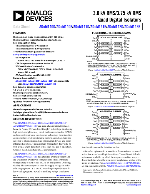
High common-mode transient immunity: 100 kV/μs V 1 ADuM140D/ADuM140E
DD1 16 VDD2
High robustness to radiated and conducted noise
GND 2
1 15 GND2
Low propagation delay
V 3 ENCODE DECODE 14
IA VOA
13 ns maximum for 5 V operation
VIB 4 ENCODE DECODE 13 VOB
15 ns maximum for 1.8 V operation
VIC 5 ENCODE DECODE 12 VOC
150 Mbps maximum guaranteed data rate
VID 6 ENCODE DECODE 11 VOD
Safety and regulatory approvals
DISABLE /NIC 7 10 NIC/VE2
UL recognition 1
GND1 8 9 GND2
3000 V rms/3750 V rms for 1 minute per UL 1577
NOTES
CSA Component Acceptance Notice 5A 1. NIC = NO INTERNAL CONNECTION. LEAVE THIS PIN FLOATING.
2. PIN 7 IS DISABLE AND PIN 10 IS NIC FOR THE ADuM140D, AND
VDE certificate of conformity 1
PIN 7 IS NIC AND PIN 10 IS VE2 FOR THE ADuM140E.
DIN V VDE V 0884-11 (VDE V 0884-11):2017-01 Figure 1. ADuM140D/ADuM140E Functional Block Diagram
VIORM = 849 V peak
CQC certification per GB4943.1-2011 V 1 ADuM141D/ADuM141E
DD1 16 VDD2
Backward compatibility GND 2
1 15 GND2
ADuM140E1/ADuM141E1/ADuM142E1 pin-compatible V 3 ENCODE DECODE 14
IA VOA
with ADuM1400/ADuM1401/ADuM1402 VIB 4 ENCODE DECODE 13 VOB
Low dynamic power consumption VIC 5 ENCODE DECODE 12 VOC
1.8 V to 5 V level translation VOD 6 DECODE ENCODE 11 VID
High temperature operation: 125°C
DISABLE1/VE1 7 10 DISABLE2/VE2
Fail-safe high or low options
GND1 8 9 GND2
16-lead, RoHS compliant, SOIC package
NOTES
Qualified for automotive applications 1. PIN 7 IS DISABLE1 AND PIN 10 IS DISABLE2 FOR THE ADuM141D,
AND PIN 7 IS VE1 AND PIN 10 IS VE2 FOR THE ADuM141E.
APPLICATIONS
Figure 2. ADuM141D/ADuM141E Functional Block Diagram
General-purpose multichannel isolation
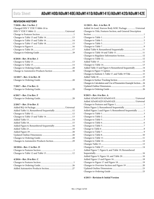
Serial peripheral interface (SPI)/data converter isolation V 1 ADuM142D/ADuM142E
DD1 16 VDD2
Industrial field bus isolation GND 2
1 15 GND2
V 3 ENCODE DECODE 14
GENERAL DESCRIPTION IA VOA
VIB 4 ENCODE DECODE 13 VOB
The ADuM140D/ADuM140E/ADuM141D/ADuM141E/
VOC 5 DECODE ENCODE 12 VIC
ADuM142D/ADuM142E1 are quad-channel digital isolators
VOD 6 11 VID
based on Analog Devices, Inc., iCoupler® technology. Combining DECODE ENCODE
DISABLE /V 7 10 DISABLE /V
high speed, complementary metal-oxide semiconductor (CMOS) 1 E1 2 E2
GND 8 9 GND
and monolithic air core transformer technology, these isolation 1 2
NOTES
components provide outstanding performance characteristics 1. PIN 7 IS DISABLE1 AND PIN 10 IS DISABLE2 FOR THE ADuM142D,
superior to alternatives such as optocoupler devices and other AND PIN 7 IS VE1 AND PIN 10 IS VE2 FOR THE ADuM142E.
integrated couplers. The maximum propagation delay is 13 ns Figure 3. ADuM142D/ADuM142E Functional Block Diagram
with a pulse width distortion of less than 3 ns at 5 V operation. functionality across the isolation barrier.
Channel matching is tight at 3.0 ns maximum. Unlike other optocoupler alternatives, dc correctness is ensured
The ADuM140D/ADuM140E/ADuM141D/ADuM141E/ in the absence of input logic transitions. Two different fail-safe
ADuM142D/ADuM142E data channels are independent and options are available, by which the outputs transition to a pre-
are available in a variety of configurations with a withstand determined state when the input power supply is not applied or the
voltage rating of 3.0 kV rms or 3.75 kV rms (see the Ordering inputs are disabled. The ADuM140E1/ADuM141E1/ADuM142E1
Guide). The devices operate with the supply voltage on either are pin-compatible with the ADuM1400/ADuM1401/ADuM1402.
side ranging from 1.8 V to 5 V, providing compatibility with
1 Protected by U.S. Patents 5,952,849; 6,873,065; 6,903,578; and 7,075,329.
lower voltage systems as well as enabling voltage translation Other patents are pending.
Rev. J Document Feedback
Information furnished by Analog Devices is believed to be accurate and reliable. However, no
responsibility is assumed by Analog Devices for its use, nor for any infringements of patents or other
rights of third parties that may result from its use. Specifications subject to change without notice. One Technology Way, P.O. Box 9106, Norwood, MA 02062-9106, U.S.A.
No license is granted by implication or otherwise under any patent or patent rights of Analog Tel: 781.329.4700 ©2015–2020 Analog Devices, Inc. All rights reserved.
Devices. Trademarks and registered trademarks are the property of their respective owners. Technical Support www.analog.com
13119-103 13119-102 13119-101
Page2
TABLE OF CONTENTS
ADuM140D/ADuM140E/ADuM141D/ADuM141E/ADuM142D/ADuM142E Data Sheet
TABLE OF CONTENTS
Features .............................................................................................. 1 Absolute Maximum Ratings ......................................................... 17
Applications ...................................................................................... 1 ESD Caution ............................................................................... 17
General Description ......................................................................... 1 Truth Tables ................................................................................ 18
Functional Block Diagrams ............................................................. 1 Pin Configurations and Function Descriptions ......................... 19
Revision History ............................................................................... 3 Typical Performance Characteristics .......................................... 22
Specifications .................................................................................... 4 Applications Information ............................................................. 24
Electrical Characteristics—5 V Operation ................................ 4 Overview ...................................................................................... 24
Electrical Characteristics—3.3 V Operation ............................ 6 Printed Circuit Board (PCB) Layout ....................................... 24
Electrical Characteristics—2.5 V Operation ............................ 8 Propagation Delay Related Parameters ................................... 25
Electrical Characteristics—1.8 V Operation .......................... 10 Jitter Measurement .................................................................... 25
Insulation and Safety Related Specifications .......................... 12 Insulation Lifetime ..................................................................... 25
Package Characteristics ............................................................. 12 Outline Dimensions ....................................................................... 27
Regulatory Information ............................................................. 13 Ordering Guide .......................................................................... 28
DIN V VDE V 0884-11 (VDE V 0884-11) Insulation Automotive Products ................................................................ 30
Characteristics ............................................................................ 14
Recommended Operating Conditions .................................... 16
Rev. J | Page 2 of 30
Page3
REVISION HISTORY
Data Sheet ADuM140D/ADuM140E/ADuM141D/ADuM141E/ADuM142D/ADuM142E
REVISION HISTORY
7/2020—Rev. I to Rev. J 11/2015—Rev. A to Rev. B
Changed DIN V VDE V 0884-10 to Added 16-Lead, Narrow Body SOIC Package ............... Universal
DIN V VDE V 0884-11 ..................................................... Universal Changes to Title, Features Section, and General Description
Change to Features Section ............................................................. 1 Section ................................................................................................ 1
Changes to Table 13 and Table 14 ................................................ 13 Changes to Table 1 ............................................................................ 3
Changes to Table 15 and Table 16 ................................................ 14 Changes to Table 3 ............................................................................ 5
Changes to Table 17 and Table 18 ................................................ 15 Changes to Table 5 ............................................................................ 7
Changes to Figure 6 ........................................................................ 16 Changes to Table 7 ............................................................................ 9
Changes to Table 20 ........................................................................ 17 Added Table 9; Renumbered Sequentially .................................. 11
Changes to Ordering Guide .................................................................. 29 Changes to Table 10 and Table 11 ................................................ 11
Changes to Regulator Information Section ................................. 12
8/2018—Rev. H to Rev. I Changes to Table 12 ........................................................................ 12
Changes to Table 13 ........................................................................ 13 Added Table 13 ............................................................................... 12
Changes to Table 15 ........................................................................ 14 Changes to Table 14 ........................................................................ 13
Changes to Ordering Guide ........................................................... 28 Added Table 15 and Figure 4; Renumbered Sequentially ............... 14
Change to Automotive Products Section .................................... 30 Changes to Figure 5 Caption ................................................................. 14
Changes to Endnote 3, Table 17, and Table 19 Title ........................ 15
12/2017—Rev. G to Rev. H Added Table 18 ........................................................................................ 15
Changes to Ordering Guide ........................................................... 28 Changes to Surface Tracking Section .................................................. 23
Changes to Calculation and Use of Parameters Example Section .... 24
7/2017—Rev. F to Rev. G Updated Outline Dimensions ............................................................... 25
Changes to Ordering Guide ........................................................... 28 Changes to Ordering Guide .................................................................. 26
6/2017—Rev. E to Rev. F 9/2015—Rev. 0 to Rev. A
Changes to Ordering Guide ........................................................... 28 Added ADuM141D/ADuM141E ..................................... Universal
Added ADuM142D/ADuM142E ..................................... Universal
2/2017—Rev. D to Rev. E Changes to Features and Figure 1 ................................................... 1
Added RQ-16 Package ....................................................... Universal Delete Figure 2; Renumbered Sequentially ................................... 1
Added Table 11; Renumbered Sequentially ................................ 12 Added Figure 2 and Figure 3; Renumbered Sequentially ........... 1
Changes to Table 12 ........................................................................ 12 Changes to Table 1 ............................................................................ 3
Changes to Table 13 and Table 14 ................................................ 13 Changes to Table 2 ............................................................................ 4
Added Table 15 ................................................................................ 14 Changes to Table 3 ............................................................................ 5
Added Table 18 ................................................................................ 15 Changes to Table 4 ............................................................................ 6
Added Figure 6; Renumbered Sequentially ................................. 16 Changes to Table 5 ............................................................................ 7
Added Table 23 ................................................................................ 18 Change to Table 6 ............................................................................. 8
Added Figure 29 .............................................................................. 28 Changes to Table 7 ............................................................................ 9
Updated Outline Dimensions ....................................................... 28 Changes to Table 8 .......................................................................... 10
Changes to Ordering Guide ........................................................... 28 Changes to Table 11 ........................................................................ 11
Changes to Automotive Products Section ................................... 29 Changes to Table 12 ........................................................................ 12
Changes Table 15 ............................................................................ 13
10/2016—Rev. C to Rev. D Changes to Table 17 ........................................................................ 14
Changes to Features Section ............................................................ 1 Added Figure 7, Figure 8, and Table 19; Renumbered
Changes to Table 12 and Table 13 ................................................ 12 Sequentially ...................................................................................... 16
Added Figure 9, Figure 10, and Table 20 ..................................... 16
4/2016—Rev. B to Rev. C Added Figure 13 and Figure 16 ..................................................... 18
Changes to Features Section ............................................................ 1 Changes to Figure 17 and Figure 18 ............................................. 19
Changes to Ordering Guide ........................................................... 26 Changes to Overview Section and Figure 19 .............................. 20
Added Automotive Products Section ........................................... 27 Updated Outline Dimensions ....................................................... 23
Changes to Ordering Guide .......................................................... 23
4/2015—Revision 0: Initial Version
Rev. J | Page 3 of 30
Page4
SPECIFICATIONS、ELECTRICAL CHARACTERISTICS—5 V OPERATION
ADuM140D/ADuM140E/ADuM141D/ADuM141E/ADuM142D/ADuM142E Data Sheet
SPECIFICATIONS
ELECTRICAL CHARACTERISTICS—5 V OPERATION
All typical specifications are at TA = 25°C, VDD1 = VDD2 = 5 V. Minimum/maximum specifications apply over the entire recommended
operation range of 4.5 V ≤ VDD1 ≤ 5.5 V, 4.5 V ≤ VDD2 ≤ 5.5 V, and −40°C ≤ TA ≤ +125°C, unless otherwise noted. Switching specifications
are tested with CL = 15 pF and CMOS signal levels, unless otherwise noted. Supply currents are specified with 50% duty cycle signals.
Table 1.
Parameter Symbol Min Typ Max Unit Test Conditions/Comments
SWITCHING SPECIFICATIONS
Pulse Width PW 6.6 ns Within pulse width distortion (PWD) limit
Data Rate1 150 Mbps Within PWD limit
Propagation Delay tPHL, tPLH 4.8 7.2 13 ns 50% input to 50% output
Pulse Width Distortion PWD 0.5 3 ns |tPLH − tPHL|
Change vs. Temperature 1.5 ps/°C
Propagation Delay Skew tPSK 6.1 ns Between any two units at the
same temperature, voltage, and load
Channel Matching
Codirectional tPSKCD 0.5 3.0 ns
Opposing Direction tPSKOD 0.5 3.0 ns
Jitter 490 ps p-p See the Jitter Measurement section
70 ps rms See the Jitter Measurement section
DC SPECIFICATIONS
Input Threshold Voltage
Logic High VIH 0.7 × VDDx V
Logic Low VIL 0.3 × VDDx V
Output Voltage
Logic High VOH VDDx − 0.1 VDDx V I 2
Ox = −20 μA, VIx = V 3
IxH
V 2 3
DDx − 0.4 VDDx − V IOx = −4 mA, VIx = VIxH
0.2
Logic Low VOL 0.0 0.1 V I 2 4
Ox = 20 μA, VIx = VIxL
0.2 0.4 V I 2 = 4 mA, V = V 4
Ox Ix IxL
Input Current per Channel II −10 +0.01 +10 μA 0 V ≤ VIx ≤ VDDx
VE2 Enable Input Pull-Up Current IPU −10 −3 μA VE2 = 0 V
DISABLE1 Input Pull-Down Current IPD 9 15 μA DISABLE1 = VDDx
Tristate Output Current per Channel IOZ −10 +0.01 +10 μA 0 V ≤ VOx ≤ VDDx
Quiescent Supply Current
ADuM140D/ADuM140E
IDD1 (Q) 1.2 2.2 mA V 5
I = 0 (E0, D0), 1 (E1, D1)6
I 5
DD2 (Q) 2.0 2.72 mA VI = 0 (E0, D0), 1 (E1, D1)6
IDD1 (Q) 12.0 20.0 mA V 5
I = 1 (E0, D0), 0 (E1, D1)6
IDD2 (Q) 2.0 2.92 mA V 5
I = 1 (E0, D0), 0 (E1, D1)6
ADuM141D/ADuM141E
I 5 6
DD1 (Q) 1.6 2.46 mA VI = 0 (E0, D0), 1 (E1, D1)
I 5 6
DD2 (Q) 1.9 2.62 mA VI = 0 (E0, D0), 1 (E1, D1)
I 5 6
DD1 (Q) 10.0 17.0 mA VI = 1 (E0, D0), 0 (E1, D1)
IDD2 (Q) 6.0 10.0 mA V 5
I = 1 (E0, D0), 0 (E1, D1)6
ADuM142D/ADuM142E
I 1.6 2.46 mA V 5
DD1 (Q) I = 0 (E0, D0), 1 (E1, D1)6
I 5 6
DD2 (Q) 1.6 2.46 mA VI = 0 (E0, D0), 1 (E1, D1)
I 5 6
DD1 (Q) 7.2 11.5 mA VI = 1 (E0, D0), 0 (E1, D1)
IDD2 (Q) 8.4 11.5 mA V 5
I = 1 (E0, D0), 0 (E1, D1)6
Rev. J | Page 4 of 30
Page5
Data Sheet ADuM140D/ADuM140E/ADuM141D/ADuM141E/ADuM142D/ADuM142E
Parameter Symbol Min Typ Max Unit Test Conditions/Comments
Dynamic Supply Current
Dynamic Input IDDI (D) 0.01 mA/Mbps Inputs switching, 50% duty cycle
Dynamic Output IDDO (D) 0.02 mA/Mbps Inputs switching, 50% duty cycle
Undervoltage Lockout UVLO
Positive VDDx Threshold VDDxUV+ 1.6 V
Negative VDDx Threshold VDDxUV− 1.5 V
VDDx Hysteresis VDDxUVH 0.1 V
AC SPECIFICATIONS
Output Rise/Fall Time tR/tF 2.5 ns 10% to 90%
Common-Mode Transient |CMH| 75 100 kV/μs VIx = VDDx, VCM = 1000 V,
Immunity7 transient magnitude = 800 V
|CML| 75 100 kV/μs VIx = 0 V, VCM = 1000 V,
transient magnitude = 800 V
1 150 Mbps is the highest data rate that can be guaranteed, although higher data rates are possible.
2 IOx is the Channel x output current, where x = A, B, C, or D.
3 VIxH is the input side logic high.
4 VIxL is the input side logic low.
5 VI is the voltage input.
6 E0 is the ADuM140E0/ADuM141E0/ADuM142E0 models, D0 is the ADuM140D0/ADuM141D0/ADuM142D0 models, E1 is the ADuM140E1/ADuM141E1/ADuM142E1
models, and D1 is the ADuM140D1/ADuM141D1/ADuM142D1 models. See the Ordering Guide section.
7 |CMH| is the maximum common-mode voltage slew rate that can be sustained while maintaining the voltage output (VO) > 0.8 VDDx. |CML| is the maximum common-
mode voltage slew rate that can be sustained while maintaining VO > 0.8 V. The common-mode voltage slew rates apply to both rising and falling common-mode
voltage edges.
Table 2. Total Supply Current vs. Data Throughput
1 Mbps 25 Mbps 100 Mbps
Parameter Symbol Min Typ Max Min Typ Max Min Typ Max Unit
SUPPLY CURRENT
ADuM140D/ADuM140E
Supply Current Side 1 IDD1 6.8 10 7.8 12 11.8 17.4 mA
Supply Current Side 2 IDD2 2.1 3.7 3.9 5.7 9.2 13 mA
ADuM141D/ADuM141E
Supply Current Side 1 IDD1 5.8 10.3 7.0 10.9 11.4 15.9 mA
Supply Current Side 2 IDD2 4.0 6.85 5.5 8.5 10.3 14.0 mA
ADuM142D/ADuM142E
Supply Current Side 1 IDD1 4.3 7.7 6.0 9.3 10.3 14.2 mA
Supply Current Side 2 IDD2 5.3 8.7 6.7 10.1 11.0 14.9 mA
Rev. J | Page 5 of 30
Page6
ELECTRICAL CHARACTERISTICS—3.3 V OPERATION
ADuM140D/ADuM140E/ADuM141D/ADuM141E/ADuM142D/ADuM142E Data Sheet
ELECTRICAL CHARACTERISTICS—3.3 V OPERATION
All typical specifications are at TA = 25°C, VDD1 = VDD2 = 3.3 V. Minimum/maximum specifications apply over the entire recommended
operation range: 3.0 V ≤ VDD1 ≤ 3.6 V, 3.0 V ≤ VDD2 ≤ 3.6 V, and −40°C ≤ TA ≤ +125°C, unless otherwise noted. Switching specifications
are tested with CL = 15 pF and CMOS signal levels, unless otherwise noted. Supply currents are specified with 50% duty cycle signals.
Table 3.
Parameter Symbol Min Typ Max Unit Test Conditions/Comments
SWITCHING SPECIFICATIONS
Pulse Width PW 6.6 ns Within PWD limit
Data Rate1 150 Mbps Within PWD limit
Propagation Delay tPHL, tPLH 4.8 6.8 14 ns 50% input to 50% output
Pulse Width Distortion PWD 0.7 3 ns |tPLH − tPHL|
Change vs. Temperature 1.5 ps/°C
Propagation Delay Skew tPSK 7.5 ns Between any two units at the same
temperature, voltage, and load
Channel Matching
Codirectional tPSKCD 0.7 3.0 ns
Opposing Direction tPSKOD 0.7 3.0 ns
Jitter 580 ps p-p See the Jitter Measurement section
120 ps rms See the Jitter Measurement section
DC SPECIFICATIONS
Input Threshold Voltage
Logic High VIH 0.7 × VDDx V
Logic Low VIL 0.3 × VDDx V
Output Voltage
Logic High VOH VDDx − 0.1 VDDx V I 2
Ox = −20 μA, VIx = V 3
IxH
V 2 3
DDx − 0.4 VDDx − 0.2 V IOx = −2 mA, VIx = VIxH
Logic Low V 2 4
OL 0.0 0.1 V IOx = 20 μA, VIx = VIxL
0.2 0.4 V I 2
Ox = 2 mA, VIx = V 4
IxL
Input Current per Channel II −10 +0.01 +10 μA 0 V ≤ VIx ≤ VDDx
VE2 Enable Input Pull-Up Current IPU −10 −3 μA VE2 = 0 V
DISABLE1 Input Pull-Down Current IPD 9 15 μA DISABLE1 = VDDx
Tristate Output Current per Channel IOZ −10 +0.01 +10 μA 0 V ≤ VOx ≤ VDDx
Quiescent Supply Current
ADuM140D/ADuM140E
IDD1 (Q) 1.2 2.12 mA V 5
I = 0 (E0, D0), 1 (E1, D1)6
IDD2 (Q) 2.0 2.68 mA V 5
I = 0 (E0, D0), 1 (E1, D1)6
I 5 6
DD1 (Q) 12.0 19.6 mA VI = 1 (E0, D0), 0 (E1, D1)
IDD2 (Q) 2.0 2.8 mA V 5
I = 1 (E0, D0), 0 (E1, D1)6
ADuM141D/ADuM141E
I 5 6
DD1 (Q) 1.5 2.36 mA VI = 0 (E0, D0), 1 (E1, D1)
I 5 6
DD2 (Q) 1.8 2.52 mA VI = 0 (E0, D0), 1 (E1, D1)
IDD1 (Q) 9.8 16.7 mA V 5
I = 1 (E0, D0), 0 (E1, D1)6
IDD2 (Q) 5.7 9.7 mA V 5
I = 1 (E0, D0), 0 (E1, D1)6
ADuM142D/ADuM142E
I 1.6 2.4 mA V 5
DD1 (Q) I = 0 (E0, D0), 1 (E1, D1)6
IDD2 (Q) 1.6 2.4 mA V 5
I = 0 (E0, D0), 1 (E1, D1)6
I 5 6
DD1 (Q) 7.2 11.2 mA VI = 1 (E0, D0), 0 (E1, D1)
IDD2 (Q) 8.4 11.2 mA V 5
I = 1 (E0, D0), 0 (E1, D1)6
Rev. J | Page 6 of 30
Page7
Data Sheet ADuM140D/ADuM140E/ADuM141D/ADuM141E/ADuM142D/ADuM142E
Parameter Symbol Min Typ Max Unit Test Conditions/Comments
Dynamic Supply Current
Dynamic Input IDDI (D) 0.01 mA/Mbps Inputs switching, 50% duty cycle
Dynamic Output IDDO (D) 0.01 mA/Mbps Inputs switching, 50% duty cycle
Undervoltage Lockout UVLO
Positive VDDx Threshold VDDxUV+ 1.6 V
Negative VDDx Threshold VDDxUV− 1.5 V
VDDx Hysteresis VDDxUVH 0.1 V
AC SPECIFICATIONS
Output Rise/Fall Time tR/tF 2.5 ns 10% to 90%
Common-Mode Transient Immunity7 |CMH| 75 100 kV/μs VIx = VDDx, VCM = 1000 V,
transient magnitude = 800 V
|CML| 75 100 kV/μs VIx = 0 V, VCM = 1000 V,
transient magnitude = 800 V
1 150 Mbps is the highest data rate that can be guaranteed, although higher data rates are possible.
2 IOx is the Channel x output current, where x = A, B, C, or D.
3 VIxH is the input side logic high.
4 VIxL is the input side logic low.
5 VI is the voltage input.
6 E0 is the ADuM140E0/ADuM141E0/ADuM142E0 models, D0 is the ADuM140D0/ADuM141D0/ADuM142D0 models, E1 is the ADuM140E1/ADuM141E1/ADuM142E1
models, and D1 is the ADuM140D1/ADuM141D1/ADuM142D1 models. See the Ordering Guide section.
7 |CMH| is the maximum common-mode voltage slew rate that can be sustained while maintaining the voltage output (VO) > 0.8 VDDx. |CML| is the maximum common-
mode voltage slew rate that can be sustained while maintaining VO > 0.8 V. The common-mode voltage slew rates apply to both rising and falling common-mode
voltage edges.
Table 4. Total Supply Current vs. Data Throughput
1 Mbps 25 Mbps 100 Mbps
Parameter Symbol Min Typ Max Min Typ Max Min Typ Max Unit
SUPPLY CURRENT
ADuM140D/ADuM140E
Supply Current Side 1 IDD1 6.6 9.8 7.4 11.2 10.7 15.9 mA
Supply Current Side 2 IDD2 2.0 3.7 3.5 5.5 8.2 11.6 mA
ADuM141D/ADuM141E
Supply Current Side 1 IDD1 5.65 10.1 6.65 10.5 10.4 14.9 mA
Supply Current Side 2 IDD2 3.9 6.65 5.2 8.0 9.4 12.8 mA
ADuM142D/ADuM142E
Supply Current Side 1 IDD1 4.3 7.7 5.6 9.0 9.1 13 mA
Supply Current Side 2 IDD2 5.0 8.4 6.2 9.6 9.8 13.7 mA
Rev. J | Page 7 of 30
Page8
ELECTRICAL CHARACTERISTICS—2.5 V OPERATION
ADuM140D/ADuM140E/ADuM141D/ADuM141E/ADuM142D/ADuM142E Data Sheet
ELECTRICAL CHARACTERISTICS—2.5 V OPERATION
All typical specifications are at TA = 25°C, VDD1 = VDD2 = 2.5 V. Minimum/maximum specifications apply over the entire recommended
operation range: 2.25 V ≤ VDD1 ≤ 2.75 V, 2.25 V ≤ VDD2 ≤ 2.75 V, −40°C ≤ TA ≤ +125°C, unless otherwise noted. Switching specifications
are tested with CL = 15 pF and CMOS signal levels, unless otherwise noted. Supply currents are specified with 50% duty cycle signals.
Table 5.
Parameter Symbol Min Typ Max Unit Test Conditions/Comments
SWITCHING SPECIFICATIONS
Pulse Width PW 6.6 ns Within PWD limit
Data Rate1 150 Mbps Within PWD limit
Propagation Delay tPHL, tPLH 5.0 7.0 14 ns 50% input to 50% output
Pulse Width Distortion PWD 0.7 3 ns |tPLH − tPHL|
Change vs. Temperature 1.5 ps/°C
Propagation Delay Skew tPSK 6.8 ns Between any two units at the same
temperature, voltage, and load
Channel Matching
Codirectional tPSKCD 0.7 3.0 ns
Opposing Direction tPSKOD 0.7 3.0 ns
Jitter 800 ps p-p See the Jitter Measurement section
190 ps rms See the Jitter Measurement section
DC SPECIFICATIONS
Input Threshold Voltage
Logic High VIH 0.7 × VDDx V
Logic Low VIL 0.3 × VDDx V
Output Voltage
Logic High VOH VDDx − 0.1 VDDx V I 2
Ox = −20 μA, VIx = V 3
IxH
VDDx − 0.4 VDDx − 0.2 V I 2
Ox = −2 mA, VIx = V 3
IxH
Logic Low VOL 0.0 0.1 V I 2
Ox = 20 μA, V = V 4
Ix IxL
0.2 0.4 V I 2
Ox = 2 mA, VIx = V 4
IxL
Input Current per Channel II −10 +0.01 +10 μA 0 V ≤ VIx ≤ VDDx
VE2 Enable Input Pull-Up Current IPU −10 −3 μA VE2 = 0 V
DISABLE1 Input Pull-Down Current IPD 9 15 μA DISABLE1 = VDDx
Tristate Output Current per Channel IOZ −10 +0.01 +10 μA 0 V ≤ VOx ≤ VDDx
Quiescent Supply Current
ADuM140D/ADuM140E
I 5 6
DD1 (Q) 1.2 2.0 mA VI = 0 (E0, D0), 1 (E1, D1)
I 5 6
DD2 (Q) 2.0 2.64 mA VI = 0 (E0, D0), 1 (E1, D1)
IDD1 (Q) 1.2 19.6 mA V 5
I = 1 (E0, D0), 0 (E1, D1)6
IDD2 (Q) 2.0 2.76 mA V 5 6
I = 1 (E0, D0), 0 (E1, D1)
ADuM141D/ADuM141E
IDD1 (Q) 1.46 2.32 mA V 5
I = 0 (E0, D0), 1 (E1, D1)6
IDD2 (Q) 1.75 2.47 mA V 5
I = 0 (E0, D0), 1 (E1, D1)6
I 5
DD1 (Q) 9.7 16.6 mA VI = 1 (E0, D0), 0 (E1, D1)6
IDD2 (Q) 5.67 9.67 mA V 5
I = 1 (E0, D0), 0 (E1, D1)6
ADuM142D/ADuM142E
IDD1 (Q) 1.6 2.32 mA V 5
I = 0 (E0, D0), 1 (E1, D1)6
I 1.6 2.32 mA V 5
DD2 (Q) I = 0 (E0, D0), 1 (E1, D1)6
IDD1 (Q) 7.2 11.2 mA V 5
I = 1 (E0, D0), 0 (E1, D1)6
I 5
DD2 (Q) 8.4 11.2 mA VI = 1 (E0, D0), 0 (E1, D1)6
Dynamic Supply Current
Dynamic Input IDDI (D) 0.01 mA/Mbps Inputs switching, 50% duty cycle
Dynamic Output IDDO (D) 0.01 mA/Mbps Inputs switching, 50% duty cycle
Rev. J | Page 8 of 30
Page9
Data Sheet ADuM140D/ADuM140E/ADuM141D/ADuM141E/ADuM142D/ADuM142E
Parameter Symbol Min Typ Max Unit Test Conditions/Comments
Undervoltage Lockout
Positive VDDx Threshold VDDxUV+ 1.6 V
Negative VDDx Threshold VDDxUV− 1.5 V
VDDx Hysteresis VDDxUVH 0.1 V
AC SPECIFICATIONS
Output Rise/Fall Time tR/tF 2.5 ns 10% to 90%
Common-Mode Transient Immunity7 |CMH| 75 100 kV/μs VIx = VDDx, VCM = 1000 V,
transient magnitude = 800 V
|CML| 75 100 kV/μs VIx = 0 V, VCM = 1000 V,
transient magnitude = 800 V
1 150 Mbps is the highest data rate that can be guaranteed, although higher data rates are possible.
2 IOx is the Channel x output current, where x = A, B, C, or D.
3 VIxH is the input side logic high.
4 VIxL is the input side logic low.
5 VI is the voltage input.
6 E0 is the ADuM140E0/ADuM141E0/ADuM142E0 models, D0 is the ADuM140D0/ADuM141D0/ADuM142D0 models, E1 is the ADuM140E1/ADuM141E1/ADuM142E1
models, and D1 is the ADuM140D1/ADuM141D1/ADuM142D1 models. See the Ordering Guide section.
7 |CMH| is the maximum common-mode voltage slew rate that can be sustained while maintaining the voltage output (VO) > 0.8 VDDx. |CML| is the maximum common-
mode voltage slew rate that can be sustained while maintaining VO > 0.8 V. The common-mode voltage slew rates apply to both rising and falling common-mode
voltage edges.
Table 6. Total Supply Current vs. Data Throughput
1 Mbps 25 Mbps 100 Mbps
Parameter Symbol Min Typ Max Min Typ Max Min Typ Max Unit
SUPPLY CURRENT
ADuM140D/ADuM140E
Supply Current Side 1 IDD1 6.5 9.8 7.3 11.1 10.4 15.5 mA
Supply Current Side 2 IDD2 2.0 3.6 3.3 5.2 7.3 10.2 mA
ADuM141D/ADuM141E
Supply Current Side 1 IDD1 5.6 10.0 6.4 10.4 9.7 14.5 mA
Supply Current Side 2 IDD2 3.8 6.55 4.8 7.7 8.3 11.5 mA
ADuM142D/ADuM142E
Supply Current Side 1 IDD1 4.3 7.7 5.4 8.8 8.8 12.7 mA
Supply Current Side 2 IDD2 5.0 8.4 6.1 9.5 9.5 13.4 mA
Rev. J | Page 9 of 30
Page10
ELECTRICAL CHARACTERISTICS—1.8 V OPERATION
ADuM140D/ADuM140E/ADuM141D/ADuM141E/ADuM142D/ADuM142E Data Sheet
ELECTRICAL CHARACTERISTICS—1.8 V OPERATION
All typical specifications are at TA = 25°C, VDD1 = VDD2 = 1.8 V. Minimum/maximum specifications apply over the entire recommended
operation range: 1.7 V ≤ VDD1 ≤ 1.9 V, 1.7 V ≤ VDD2 ≤ 1.9 V, and −40°C ≤ TA ≤ +125°C, unless otherwise noted. Switching specifications
are tested with CL = 15 pF and CMOS signal levels, unless otherwise noted. Supply currents are specified with 50% duty cycle signals.
Table 7.
Parameter Symbol Min Typ Max Unit Test Conditions/Comments
SWITCHING SPECIFICATIONS
Pulse Width PW 6.6 ns Within PWD limit
Data Rate1 150 Mbps Within PWD limit
Propagation Delay tPHL, tPLH 5.8 8.7 15 ns 50% input to 50% output
Pulse Width Distortion PWD 0.7 3 ns |tPLH − tPHL|
Change vs. Temperature 1.5 ps/°C
Propagation Delay Skew tPSK 7.0 ns Between any two units at the same
temperature, voltage, and load
Channel Matching
Codirectional tPSKCD 0.7 3.0 ns
Opposing Direction tPSKOD 0.7 3.0 ns
Jitter 470 ps p-p See the Jitter Measurement section
70 ps rms See the Jitter Measurement section
DC SPECIFICATIONS
Input Threshold Voltage
Logic High VIH 0.7 × VDDx V
Logic Low VIL 0.3 × VDDx V
Output Voltage
Logic High V 2 3
OH VDDx − 0.1 VDDx V IOx = −20 μA, VIx = VIxH
V 2 3
DDx − 0.4 VDDx − 0.2 V IOx = −2 mA, VIx = VIxH
Logic Low V 2 4
OL 0.0 0.1 V IOx = 20 μA, VIx = VIxL
0.2 0.4 V I 2 4
Ox = 2 mA, VIx = VIxL
Input Current per Channel II −10 +0.01 +10 μA 0 V ≤ VIx ≤ VDDx
VE2 Enable Input Pull-Up Current IPU −10 −3 μA VE2 = 0 V
DISABLE1 Input Pull-Down Current IPD 9 15 μA DISABLE1 = VDDx
Tristate Output Current per Channel IOZ −10 +0.01 +10 μA 0 V ≤ VOx ≤ VDDx
Quiescent Supply Current
ADuM140D/ADuM140E
IDD1 (Q) 1.2 1.92 mA V 5
I = 0 (E0, D0), 1 (E1, D1)6
IDD2 (Q) 2.0 2.64 mA V 5
I = 0 (E0, D0), 1 (E1, D1)6
I 5 6
DD1 (Q) 12.0 19.6 mA VI = 1 (E0, D0), 0 (E1, D1)
IDD2 (Q) 2.0 2.76 mA V 5
I = 1 (E0, D0), 0 (E1, D1)6
ADuM141D/ADuM141E
I 5 6
DD1 (Q) 1.4 2.28 mA VI = 0 (E0, D0), 1 (E1, D1)
I 5 6
DD2 (Q) 1.73 2.45 mA VI = 0 (E0, D0), 1 (E1, D1)
IDD1 (Q) 9.6 16.5 mA V 5
I = 1 (E0, D0), 0 (E1, D1)6
IDD2 (Q) 5.6 9.6 mA V 5
I = 1 (E0, D0), 0 (E1, D1)6
ADuM142D/ADuM142E
IDD1 (Q) 1.6 2.28 mA V 5
I = 0 (E0, D0), 1 (E1, D1)6
I 5 6
DD2 (Q) 1.6 2.28 mA VI = 0 (E0, D0), 1 (E1, D1)
I 5 6
DD1 (Q) 7.2 11.2 mA VI = 1 (E0, D0), 0 (E1, D1)
IDD2 (Q) 8.4 11.2 mA V 5
I = 1 (E0, D0), 0 (E1, D1)6
Rev. J | Page 10 of 30
Page11
Data Sheet ADuM140D/ADuM140E/ADuM141D/ADuM141E/ADuM142D/ADuM142E
Parameter Symbol Min Typ Max Unit Test Conditions/Comments
Dynamic Supply Current
Dynamic Input IDDI (D) 0.01 mA/Mbps Inputs switching, 50% duty cycle
Dynamic Output IDDO (D) 0.01 mA/Mbps Inputs switching, 50% duty cycle
Undervoltage Lockout UVLO
Positive VDDx Threshold VDDxUV+ 1.6 V
Negative VDDx Threshold VDDxUV− 1.5 V
VDDx Hysteresis VDDxUVH 0.1 V
AC SPECIFICATIONS
Output Rise/Fall Time tR/tF 2.5 ns 10% to 90%
Common-Mode Transient Immunity7 |CMH| 75 100 kV/μs VIx = VDDx, VCM = 1000 V,
transient magnitude = 800 V
|CML| 75 100 kV/μs VIx = 0 V, VCM = 1000 V,
transient magnitude = 800 V
1 150 Mbps is the highest data rate that can be guaranteed, although higher data rates are possible.
2 IOx is the Channel x output current, where x = A, B, C, or D.
3 VIxH is the input side logic high.
4 VIxL is the input side logic low.
5 VI is the voltage input.
6 E0 is the ADuM140E0/ADuM141E0/ADuM142E0 models, D0 is the ADuM140D0/ADuM141D0/ADuM142D0 models, E1 is the ADuM140E1/ADuM141E1/ADuM142E1
models, and D1 is the ADuM140D1/ADuM141D1/ADuM142D1 models. See the Ordering Guide section.
7 |CMH| is the maximum common-mode voltage slew rate that can be sustained while maintaining the voltage output (VO) > 0.8 VDDx. |CML| is the maximum common-
mode voltage slew rate that can be sustained while maintaining VO > 0.8 V. The common-mode voltage slew rates apply to both rising and falling common-mode
voltage edges.
Table 8. Total Supply Current vs. Data Throughput
1 Mbps 25 Mbps 100 Mbps
Parameter Symbol Min Typ Max Min Typ Max Min Typ Max Unit
SUPPLY CURRENT
ADuM140D/ADuM140E
Supply Current Side 1 IDD1 6.4 9.8 7.2 11 10.2 15.2 mA
Supply Current Side 2 IDD2 1.9 3.5 3.1 5.0 6.8 10 mA
ADuM141D/ADuM141E
Supply Current Side 1 IDD1 5.5 9.1 6.3 10.0 9.6 14.0 mA
Supply Current Side 2 IDD2 3.72 6.45 4.8 7.5 8.4 11.2 mA
ADuM142D/ADuM142E
Supply Current Side 1 IDD1 4.3 7.7 5.3 8.7 8.6 12.6 mA
Supply Current Side 2 IDD2 4.9 8.3 6.0 9.4 9.3 13.3 mA
Rev. J | Page 11 of 30
Page12
INSULATION AND SAFETY RELATED SPECIFICATIONS、PACKAGE CHARACTERISTICS
ADuM140D/ADuM140E/ADuM141D/ADuM141E/ADuM142D/ADuM142E Data Sheet
INSULATION AND SAFETY RELATED SPECIFICATIONS
For additional information, see www.analog.com/icouplersafety.
Table 9. R-16 Narrow Body [SOIC_N] Package
Parameter Symbol Value Unit Test Conditions/Comments
Rated Dielectric Insulation Voltage 3000 V rms 1-minute duration
Minimum External Air Gap (Clearance) L (I01) 4.0 mm min Measured from input terminals to output terminals, shortest
distance through air
Minimum External Tracking (Creepage) L (I02) 4.0 mm min Measured from input terminals to output terminals, shortest
distance path along body
Minimum Clearance in the Plane of the Printed L (PCB) 4.5 mm min Measured from input terminals to output terminals, shortest
Circuit Board (PCB Clearance) distance through air, line of sight, in the PCB mounting plane
Minimum Internal Gap (Internal Clearance) 25.5 μm min Minimum distance through insulation
Tracking Resistance (Comparative Tracking Index) CTI >400 V DIN IEC 112/VDE 0303 Part 1
Material Group II Material Group (DIN VDE 0110, 1/89, Table 1)
Table 10. RW-16 Wide Body [SOIC_W] Package
Parameter Symbol Value Unit Test Conditions/Comments
Rated Dielectric Insulation Voltage 3750 V rms 1-minute duration
Minimum External Air Gap (Clearance) L (I01) 7.8 mm min Measured from input terminals to output terminals, shortest
distance through air
Minimum External Tracking (Creepage) L (I02) 7.8 mm min Measured from input terminals to output terminals, shortest
distance path along body
Minimum Clearance in the Plane of the Printed L (PCB) 8.3 mm min Measured from input terminals to output terminals, shortest
Circuit Board (PCB Clearance) distance through air, line of sight, in the PCB mounting plane
Minimum Internal Gap (Internal Clearance) 25.5 μm min Minimum distance through insulation
Tracking Resistance (Comparative Tracking Index) CTI >400 V DIN IEC 112/VDE 0303 Part 1
Material Group II Material Group (DIN VDE 0110, 1/89, Table 1)
Table 11. RQ-16 [QSOP] Package
Parameter Symbol Value Unit Test Conditions/Comments
Rated Dielectric Insulation Voltage 3000 V rms 1-minute duration
Minimum External Air Gap (Clearance) L (I01) 3.2 mm min Measured from input terminals to output terminals, shortest
distance through air
Minimum External Tracking (Creepage) L (I02) 3.2 mm min Measured from input terminals to output terminals, shortest
distance path along body
Minimum Clearance in the Plane of the Printed L (PCB) 3.8 mm min Measured from input terminals to output terminals, shortest
Circuit Board (PCB Clearance) distance through air, line of sight, in the PCB mounting plane
Minimum Internal Gap (Internal Clearance) 25.5 μm min Minimum distance through insulation
Tracking Resistance (Comparative Tracking Index) CTI >400 V DIN IEC 112/VDE 0303 Part 1
Material Group II Material Group (DIN VDE 0110, 1/89, Table 1)
PACKAGE CHARACTERISTICS
Table 12.
Parameter Symbol Min Typ Max Unit Test Conditions/Comments
Resistance (Input to Output)1 RI-O 1013 Ω
Capacitance (Input to Output)1 CI-O 2.2 pF f = 1 MHz
Input Capacitance2 CI 4.0 pF
IC Junction to Ambient Thermal Resistance
R-16 Narrow Body [SOIC_N] Package θJA 76 °C/W Thermocouple located at center of package underside
RW-16 Wide Body [SOIC_W] Package θJA 45 °C/W Thermocouple located at center of package underside
RQ-16 [QSOP] Package θJA 76 °C/W Thermocouple located at center of package underside
1 The device is considered a 2-terminal device: Pin 1 through Pin 8 are shorted together, and Pin 9 through Pin 16 are shorted together.
2 Input capacitance is from any input data pin to ground.
Rev. J | Page 12 of 30
Page13
REGULATORY INFORMATION
Data Sheet ADuM140D/ADuM140E/ADuM141D/ADuM141E/ADuM142D/ADuM142E
REGULATORY INFORMATION
See Table 21 for the SOIC_N package or Table 22 for the SOIC_W package and the Insulation Lifetime section for details regarding
recommended maximum working voltages for specific cross isolation waveforms and insulation levels.
Table 13. R-16 Narrow Body [SOIC_N] Package
UL CSA VDE CQC
Recognized Under UL 1577 Approved under CSA Component Certified according to Certified under
Component Recognition Acceptance Notice 5A DIN V VDE V 0884-11 CQC11-471543-2012
Program1 (VDE V 0884-11):2017-012
Single Protection, 3000 V rms CSA 60950-1-07+A1+A2 and IEC 60950-1, Reinforced insulation, VIORM = GB4943.1-2011:
Isolation Voltage second edition, +A1+A2: 565 V peak, VIOSM = 6000 V peak
Basic insulation at 400 V rms (565 V peak) Basic insulation, VIORM = Basic insulation at
565 V peak, VIOSM = 10 kV peak 770 V rms (1089 V peak)
Reinforced insulation at 200 V rms Reinforced insulation at
(283 V peak) 385 V rms (545 V peak)
IEC 60601-1 Edition 3.1:
Basic insulation (one means of patient
protection (1 MOPP)), 250 V rms
(354 V peak)
CSA 61010-1-12 and IEC 61010-1 third
edition:
Basic insulation at 300 V rms mains,
400 V rms secondary (565 V peak)
Reinforced insulation at 300 V rms mains,
200 V secondary (282 V peak)
File E214100 File 205078 File 2471900-4880-0001 File CQC16001147385
1 In accordance with UL 1577, each ADuM140D/ADuM140E/ADuM141D/ADuM141E/ADuM142D/ADuM142E in the R-16 narrow body [SOIC_N] package is proof tested by
applying an insulation test voltage ≥ 3600 V rms for 1 sec.
2 In accordance with DIN V VDE V 0884-11, each ADuM140D/ADuM140E/ADuM141D/ADuM141E/ADuM142D/ADuM142E in the R-16 narrow body [SOIC_N] package is
proof tested by applying an insulation test voltage ≥ 1059 V peak for 1 sec (partial discharge detection limit = 5 pC). The * marking branded on the component
designates DIN V VDE V 0884-11 approval.
Table 14. RW-16 Wide Body [SOIC_W] Package
UL CSA VDE CQC
Recognized Under UL 1577 Approved under CSA Component Certified according to Certified under
Component Recognition Acceptance Notice 5A DIN V VDE V 0884-11 CQC11-471543-2012
Program1 (VDE V 0884-11):2017-012
Single Protection, 3750 V rms CSA 60950-1-07+A1+A2 and IEC 60950-1, Reinforced insulation, VIORM = GB4943.1-2011:
Isolation Voltage second edition, +A1+A2: 849 V peak, VIOSM = 6000 V peak
Basic insulation at 780 V rms Basic insulation, VIORM = Basic insulation at
(1103 V peak) 849 V peak, VIOSM = 10 kV peak 780 V rms (1103 V peak)
Reinforced insulation at 390 V rms Reinforced insulation at
(552 V peak) 390 V rms (552 V peak)
IEC 60601-1 Edition 3.1:
Basic insulation (1 means of patient
protection (MOPP)), 490 V rms (693 V peak)
CSA 61010-1-12 and IEC 61010-1 third
edition:
Basic insulation at 300 V rms mains, 780 V
secondary (1103 V peak)
Reinforced insulation at 300 V rms mains,
390 V secondary (552 V peak)
File E214100 File 205078 File 2471900-4880-0001 File CQC16001147385
1 In accordance with UL 1577, each ADuM140D/ADuM140E/ADuM141D/ADuM141E/ADuM142D/ADuM142E in the RW-16 wide body [SOIC_W] package is proof tested by
applying an insulation test voltage ≥ 4500 V rms for 1 sec.
2 In accordance with DIN V VDE V 0884-11, each ADuM140D/ADuM140E/ADuM141D/ADuM141E/ADuM142D/ADuM142E in the RW-16 wide body [SOIC_W] package is
proof tested by applying an insulation test voltage ≥ 1592 V peak for 1 sec (partial discharge detection limit = 5 pC). The * marking branded on the component
designates DIN V VDE V 0884-11 approval.
Rev. J | Page 13 of 30
Page14
DIN V VDE V 0884-10 (VDE V 0884-10) INSULATION CHARACTERISTICS
ADuM140D/ADuM140E/ADuM141D/ADuM141E/ADuM142D/ADuM142E Data Sheet
Table 15. RQ-16 [QSOP] Package
UL CSA VDE CQC
Recognized Under UL 1577 Approved under CSA Component Certified according to DIN V VDE V Certified under
Component Recognition Acceptance Notice 5A 0884-11 (VDE V 0884-11):2017-012 CQC11-471543-2012
Program1
Single Protection, 3000 V rms CSA 60950-1-07+A1+A2 and IEC 60950-1, Reinforced insulation, 636 V peak, GB4943.1-2011:
Isolation Voltage second edition, +A1+A2: VIOSM = 6 kV peak
Basic insulation at 320 V rms (450 V peak) Basic insulation 636 V peak, Basic insulation at
VIOSM = 10 kV peak 320 V rms (450 V peak)
Reinforced insulation at 160 V rms Reinforced insulation at
(225 V peak) 160Vrms (225 Vpeak)
IEC 60601-1 Edition 3.1:
Basic insulation (1MOPP), 250 V rms
(354 V peak)
CSA 61010-1-12 and IEC 61010-1 third
edition:
Basic insulation at 300V rms mains,
320 V rms (450 V peak)
Reinforced insulation at 150 V rms mains,
160 V rms (225 V peak) secondary
File E214100 File 205078 File 2471900-4880-0001 File CQC18001192421
1 In accordance with UL 1577, each ADuM140D/ADuM140E/ADuM141D/ADuM141E/ADuM142D/ADuM142E in the RQ-16 [QSOP] package is proof tested by applying an
insulation test voltage ≥ 3600 V rms for 1 sec.
2 In accordance with DIN V VDE V 0884-11, each ADuM140D/ADuM140E/ADuM141D/ADuM141E/ADuM142D/ADuM142E in the RQ-16 [QSOP] package is proof tested by
applying an insulation test voltage ≥ 1059 V peak for 1 sec (partial discharge detection limit = 5 pC). The * marking branded on the component designates DIN V VDE V
0884-11 approval.
DIN V VDE V 0884-11 (VDE V 0884-11) INSULATION CHARACTERISTICS
These isolators are suitable for reinforced electrical isolation only within the safety limit data. Protective circuits ensure the maintenance
of the safety data. The * marking on packages denotes DIN V VDE V 0884-11 approval.
Table 16. R-16 Narrow Body [SOIC_N] Package
Description Test Conditions/Comments Symbol Characteristic Unit
Installation Classification per DIN VDE 0110
For Rated Mains Voltage ≤ 150 V rms I to IV
For Rated Mains Voltage ≤ 300 V rms I to IV
For Rated Mains Voltage ≤ 600 V rms I to III
Climatic Classification 40/125/21
Pollution Degree per DIN VDE 0110, Table 1 2
Maximum Working Insulation Voltage VIORM 565 V peak
Input to Output Test Voltage, Method B1 VIORM × 1.875 = Vpd (m), 100% production test, Vpd (m) 1059 V peak
tini = tm = 1 sec, partial discharge < 5 pC
Input to Output Test Voltage, Method A Vpd (m)
After Environmental Tests Subgroup 1 VIORM × 1.5 = Vpd (m), tini = 60 sec, tm = 10 sec, 848 V peak
partial discharge < 5 pC
After Input and/or Safety Test Subgroup 2 VIORM × 1.2 = Vpd (m), tini = 60 sec, tm = 10 sec, 678 V peak
and Subgroup 3 partial discharge < 5 pC
Highest Allowable Overvoltage VIOTM 4200 V peak
Surge Isolation Voltage Basic V peak = 10 kV, 1.2 μs rise time, 50 μs, VIOSM 10000 V peak
50% fall time
Surge Isolation Voltage Reinforced V peak = 10 kV, 1.2 μs rise time, 50 μs, VIOSM 6000 V peak
50% fall time
Safety Limiting Values per VDE certification Maximum value allowed in the event of a failure
(see Figure 4)
Maximum Junction Temperature TS 150 °C
Total Power Dissipation at 25°C PS 1.64 W
Insulation Resistance at TS VIO = 500 V RS >109 Ω
Rev. J | Page 14 of 30
Page15
Data Sheet ADuM140D/ADuM140E/ADuM141D/ADuM141E/ADuM142D/ADuM142E
Table 17. RW-16 Wide Body [SOIC_W] Package
Description Test Conditions/Comments Symbol Characteristic Unit
Installation Classification per DIN VDE 0110
For Rated Mains Voltage ≤ 150 V rms I to IV
For Rated Mains Voltage ≤ 300 V rms I to IV
For Rated Mains Voltage ≤ 600 V rms I to IV
Climatic Classification 40/125/21
Pollution Degree per DIN VDE 0110, Table 1 2
Maximum Working Insulation Voltage VIORM 849 V peak
Input to Output Test Voltage, Method B1 VIORM × 1.875 = Vpd (m), 100% production test, Vpd (m) 1592 V peak
tini = tm = 1 sec, partial discharge < 5 pC
Input to Output Test Voltage, Method A Vpd (m)
After Environmental Tests Subgroup 1 VIORM × 1.5 = Vpd (m), tini = 60 sec, tm = 10 sec, 1274 V peak
partial discharge < 5 pC
After Input and/or Safety Test Subgroup 2 VIORM × 1.2 = Vpd (m), tini = 60 sec, tm = 10 sec, 1019 V peak
and Subgroup 3 partial discharge < 5 pC
Highest Allowable Overvoltage VIOTM 7000 V peak
Surge Isolation Voltage Basic V peak = 12.8 kV, 1.2 μs rise time, 50 μs, VIOSM 12000 V peak
50% fall time
Surge Isolation Voltage Reinforced V peak = 12.8 kV, 1.2 μs rise time, 50 μs, VIOSM 8000 V peak
50% fall time
Safety Limiting Values per VDE certification Maximum value allowed in the event of a failure
(see Figure 5)
Maximum Junction Temperature TS 150 °C
Total Power Dissipation at 25°C PS 2.78 W
Insulation Resistance at TS VIO = 500 V RS >109 Ω
Table 18. RQ-16 [QSOP] Package
Description Test Conditions/Comments Symbol Characteristic Unit
Installation Classification per DIN VDE 0110
For Rated Mains Voltage ≤ 150 V rms I to IV
For Rated Mains Voltage ≤ 300 V rms I to IV
For Rated Mains Voltage ≤ 600 V rms I to IV
Climatic Classification 40/125/21
Pollution Degree per DIN VDE 0110, Table 1 2
Maximum Working Insulation Voltage VIORM 565 V peak
Input to Output Test Voltage, Method B1 VIORM × 1.875 = Vpd (m), 100% production test, Vpd (m) 1059 V peak
tini = tm = 1 sec, partial discharge < 5 pC
Input to Output Test Voltage, Method A Vpd (m)
After Environmental Tests Subgroup 1 VIORM × 1.5 = Vpd (m), tini = 60 sec, tm = 10 sec, 848 V peak
partial discharge < 5 pC
After Input and/or Safety Test Subgroup 2 VIORM × 1.2 = Vpd (m), tini = 60 sec, tm = 10 sec, 678 V peak
and Subgroup 3 partial discharge < 5 pC
Highest Allowable Overvoltage VIOTM 4242 V peak
Surge Isolation Voltage Basic V peak = 10 kV, 1.2 μs rise time, 50 μs, VIOSM 10000 V peak
50% fall time
Surge Isolation Voltage Reinforced V peak = 10 kV, 1.2 μs rise time, 50 μs, VIOSM 6000 V peak
50% fall time
Safety Limiting Values per VDE certification Maximum value allowed in the event of a failure
(see Figure 5)
Maximum Junction Temperature TS 150 °C
Total Power Dissipation at 25°C PS 1.64 W
Insulation Resistance at T 9
S VIO = 500 V RS >10 Ω
Rev. J | Page 15 of 30
Page16
RECOMMENDED OPERATING CONDITIONS
ADuM140D/ADuM140E/ADuM141D/ADuM141E/ADuM142D/ADuM142E Data Sheet
4.0
1.8 SAFETY LIMITING PER
DECOMPOSITION
1.6 3.5 SAFETY LIMITING PER DIN V
VDE 0884-10
1.4 3.0
1.2 2.5
1.0
2.0
0.8
1.5
0.6
1.0
0.4
0.5
0.2
0
0 0 50 100 150 200 250 300
0 50 100 150 200
AMBIENT TEMPERATURE (°C)
AMBIENT TEMPERATURE (°C)
Figure 4. Thermal Derating Curve for R-16 Narrow Body [SOIC_N] Package, Figure 6. Thermal Derating Curve for RQ-16 [QSOP] Package,
Dependence of Safety Limiting Values with Ambient Temperature per Dependence of Safety Limiting Values with Ambient Temperature
DIN V VDE V 0884-11 RECOMMENDED OPERATING CONDITIONS
3.0 Table 19.
Parameter Symbol Rating
2.5 Operating Temperature TA −40°C to +125°C
Supply Voltages VDD1, VDD2 1.7 V to 5.5 V
2.0 Input Signal Rise and Fall Times 1.0 ms
1.5
1.0
0.5
0
0 50 100 150 200
AMBIENT TEMPERATURE (°C)
Figure 5. Thermal Derating Curve for RW-16 Wide Body [SOIC_W] Package,
Dependence of Safety Limiting Values with Ambient Temperature per
DIN V VDE V 0884-11
Rev. J | Page 16 of 30
SAFE OPERATING P , P OR P POWER (W)
SAFE LIMITING POWER (W) VDD1 VDDA VDDB
13119-003
13119-202
SAFE LIMITING POWER (W)
13119-203
Page17
ABSOLUTE MAXIMUM RATINGS、ESD CAUTION
Data Sheet ADuM140D/ADuM140E/ADuM141D/ADuM141E/ADuM142D/ADuM142E
ABSOLUTE MAXIMUM RATINGS
TA = 25°C, unless otherwise noted. Stresses at or above those listed under Absolute Maximum
Table 20. Ratings may cause permanent damage to the product. This is a
Parameter Rating stress rating only; functional operation of the product at these
or any other conditions above those indicated in the
Storage Temperature (TST) Range −65°C to +150°C
operational section of this specification is not implied.
Ambient Operating Temperature −40°C to +125°C
(T ) Range Operation beyond the maximum operating conditions for
A
Maximum Fault Junction 150°C extended periods may affect product reliability.
Temperature (TJ) per DIN V ESD CAUTION
VDE V 0884-11
Maximum Fault Junction 300°C
Temperature (TJ) per Mold
Compound
Supply Voltages (VDD1, VDD2) −0.5 V to +7.0 V
Input Voltages (VIA, VIB, VIC, VID, VE1, −0.5 V to V 1
DDI + 0.5 V
VE2, DISABLE1, DISABLE2)
Output Voltages (VOA, V 2
OB, VOC, VOD) −0.5 V to VDDO + 0.5 V
Average Output Current per Pin3
Side 1 Output Current (IO1) −10 mA to +10 mA
Side 2 Output Current (IO2) −10 mA to +10 mA
Common-Mode Transients4 −150 kV/μs to +150 kV/μs
1 VDDI is the input side supply voltage.
2 VDDO is the output side supply voltage.
3 See Figure 4 for the R-16 narrow body [SOIC_N] package, Figure 5 for the
RW-16 wide body [SOIC_W] package, or Figure 6 for the RQ-16 [QSOP]
package for the maximum rated current values at various temperatures.
4 Refers to the common-mode transients across the insulation barrier.
Common-mode transients exceeding the absolute maximum ratings may
cause latch-up or permanent damage.
Table 21. Maximum Continuous Working Voltage R-16 Narrow Body [SOIC_N] Package1
Parameter Rating Constraint2
AC Voltage
Bipolar Waveform
Basic Insulation 789 V Lifetime limited by package creepage maximum approved working voltage per IEC 60950-1
peak
Reinforced Insulation 403 V Lifetime limited by package creepage maximum approved working voltage per IEC 60950-1
peak
Unipolar Waveform
Basic Insulation 909 V Lifetime limited by package creepage maximum approved working voltage per IEC 60950-1
peak
Reinforced Insulation 469 V Lifetime limited by package creepage maximum approved working voltage per IEC 60950-1
peak
DC Voltage
Basic Insulation 558 V Lifetime limited by package creepage maximum approved working voltage per IEC 60950-1
peak
Reinforced Insulation 285V peak Lifetime limited by package creepage maximum approved working voltage per IEC 60950-1
1 Refers to the continuous voltage magnitude imposed across the isolation barrier. See the Insulation Lifetime section for more details.
2 Insulation lifetime for the specified test condition is greater than 50 years.
Table 22. Maximum Continuous Working Voltage RW-16 Wide Body [SOIC_W] Package1
Parameter Rating Constraint2
AC Voltage
Bipolar Waveform
Basic Insulation 849 V peak 50-year minimum insulation lifetime
Reinforced Insulation 768 V peak Lifetime limited by package creepage maximum approved working voltage per IEC 60950-1
Rev. J | Page 17 of 30
Page18
TRUTH TABLES
ADuM140D/ADuM140E/ADuM141D/ADuM141E/ADuM142D/ADuM142E Data Sheet
Parameter Rating Constraint2
Unipolar Waveform
Basic Insulation 1698 V peak 50-year minimum insulation lifetime
Reinforced Insulation 885 V peak Lifetime limited by package creepage maximum approved working voltage per IEC 60950-1
DC Voltage
Basic Insulation 1092 V peak Lifetime limited by package creepage maximum approved working voltage per IEC 60950-1
Reinforced Insulation 543 V peak Lifetime limited by package creepage maximum approved working voltage per IEC 60950-1
1 Refers to the continuous voltage magnitude imposed across the isolation barrier. See the Insulation Lifetime section for more details.
2 Insulation lifetime for the specified test condition is greater than 50 years.
Table 23. Maximum Continuous Working Voltage RQ-16 [QSOP] Package1
Parameter Rating Constraint2
AC Voltage
Bipolar Waveform
Basic Insulation 636 V peak Lifetime limited by package creepage maximum approved working voltage per IEC 60950-1
Reinforced Insulation 318 V peak Lifetime limited by package creepage maximum approved working voltage per IEC 60950-1
Unipolar Waveform
Basic Insulation 734 V peak Lifetime limited by package creepage maximum approved working voltage per IEC 60950-1
Reinforced Insulation 367 V peak Lifetime limited by package creepage maximum approved working voltage per IEC 60950-1
DC Voltage
Basic Insulation 450 V peak Lifetime limited by package creepage maximum approved working voltage per IEC 60950-1
Reinforced Insulation 225 V peak Lifetime limited by package creepage maximum approved working voltage per IEC 60950-1
1 Refers to the continuous voltage magnitude imposed across the isolation barrier. See the Insulation Lifetime section for more details.
2 Insulation lifetime for the specified test condition is greater than 50 years.
TRUTH TABLES
Table 24. ADuM140D/ADuM141D/ADuM142D Truth Table (Positive Logic)
Default Low (D0), Default High (D1),
VIx Input1, 2 V 1, 2
DISABLEx Input VDDI State2 V State2 V Output1, 2, 3
DDO Ox VOx Output1, 2, 3 Test Conditions/Comments
L L or NC Powered Powered L L Normal operation
H L or NC Powered Powered H H Normal operation
X H Powered Powered L H Inputs disabled, fail-safe
output
X4 X4 Unpowered Powered L H Fail-safe output
X4 X4 Powered Unpowered Indeterminate Indeterminate
1 L means low, H means high, X means don’t care, and NC means not connected.
2 VIx and VOx refer to the input and output signals of a given channel (A, B, C, or D). VDISABLEx refers to the input disable signal on the same side as the VIx inputs. VDDI and
VDDO refer to the supply voltages on the input and output sides of the given channel, respectively.
3 D0 is the ADuM140D0/ADuM141D0/ADuM142D0 models, and D1 is the ADuM140D1/ADuM141D1/ADuM142D1 models. See the Ordering Guide section.
4 Input pins (VIx, DISABLE1, and DISABLE2) on the same side as an unpowered supply must be in a low state to avoid powering the device through its ESD protection
circuitry.
Table 25. ADuM140E/ADuM141E/ADuM142E Truth Table (Positive Logic)
Default Low (E0), Default High (E1),
V Input1, 2 1, 2 2
Ix VEx Input VDDI State VDDO State2 VOx Output1, 2, 3 V 1, 2, 3
Ox Output Test Conditions/Comments
L H or NC Powered Powered L L Normal operation
H H or NC Powered Powered H H Normal operation
X L Powered Powered Z Z Outputs disabled
L H or NC Unpowered Powered L H Fail-safe output
X4 L4 Unpowered Powered Z Z Outputs disabled
X4 X4 Powered Unpowered Indeterminate Indeterminate
1 L means low, H means high, X means don’t care, NC means not connected, and Z means high impedance.
2 VIx and VOx refer to the input and output signals of a given channel (A, B, C, or D). VEx refers to the output enable signal on the same side as the VOx outputs. VDDI and
VDDO refer to the supply voltages on the input and output sides of the given channel, respectively.
3 E0 is the ADuM140E0/ADuM141E0/ADuM142E0 models, and E1 is the ADuM140E1/ADuM141E1/ADuM142E1 models. See the Ordering Guide section.
4 Input pins (VIx, VE1, and VE2) on the same side as an unpowered supply must be in a low state to avoid powering the device through its ESD protection circuitry.
Rev. J | Page 18 of 30
Page19
PIN CONFIGURATIONS AND FUNCTION DESCRIPTIONS
Data Sheet ADuM140D/ADuM140E/ADuM141D/ADuM141E/ADuM142D/ADuM142E
PIN CONFIGURATIONS AND FUNCTION DESCRIPTIONS
VDD1 1 16 VDD2 VDD1 1 16 VDD2
GND1 2 15 GND2 GND1 2 15 GND2
VIA 3 14 VOA VIA 3 14 VOA
VIB 4 ADuM140D 13 V ADuM140E
OB VIB 4 13 VOB
TOP VIEW TOP VIEW
VIC 5 (Not to Scale) 12 VOC VIC 5 (Not to Scale) 12 VOC
VID 6 11 VOD VID 6 11 VOD
DISABLE1 7 10 NIC NIC 7 10 VE2
GND1 8 9 GND2 GND1 8 9 GND2
NOTES NOTES
1. NIC = NO INTERNAL CONNECTION. 1. NIC = NO INTERNAL CONNECTION.
LEAVE THIS PIN FLOATING. LEAVE THIS PIN FLOATING.
Figure 7. ADuM140D Pin Configuration Figure 8. ADuM140E Pin Configuration
Table 26. Pin Function Descriptions
Pin No.1
ADuM140D ADuM140E Mnemonic Description
1 1 VDD1 Supply Voltage for Isolator Side 1.
2, 8 2, 8 GND1 Ground Reference for Isolator Side 1.
3 3 VIA Logic Input A.
4 4 VIB Logic Input B.
5 5 VIC Logic Input C.
6 6 VID Logic Input D.
7 Not applicable DISABLE1 Input Disable 1. This pin disables the isolator inputs. Outputs take on the logic state
determined by the fail-safe option shown in the Ordering Guide.
9, 15 9, 15 GND2 Ground Reference for Isolator Side 2.
10 7 NIC No Internal Connection. Leave this pin floating.
Not applicable 10 VE2 Output Enable 2. Active high logic input. When VE2 is high or disconnected, the VOA, VOB,
VOC, and VOD outputs are enabled. When VE2 is low, the VOA, VOB, VOC, and VOD outputs
are disabled to the high-Z state.
11 11 VOD Logic Output D.
12 12 VOC Logic Output C.
13 13 VOB Logic Output B.
14 14 VOA Logic Output A.
16 16 VDD2 Supply Voltage for Isolator Side 2.
1 Reference the AN-1109 Application Note for specific layout guidelines.
Rev. J | Page 19 of 30
13119-004
13119-005
Page20
ADuM140D/ADuM140E/ADuM141D/ADuM141E/ADuM142D/ADuM142E Data Sheet
VDD1 1 16 VDD2 VDD1 1 16 VDD2
GND1 2 15 GND2 GND1 2 15 GND2
VIA 3 14 VOA VIA 3 14 VOA
VIB 4 ADuM141D 13 VOB VIB 4 ADuM141E 13 VOB
TOP VIEW TOP VIEW
VIC 5 (Not to Scale) 12 VOC VIC 5 (Not to Scale) 12 VOC
VOD 6 11 VID VOD 6 11 VID
DISABLE1 7 10 DISABLE2 VE1 7 10 VE2
GND1 8 9 GND2 GND1 8 9 GND2
Figure 9. ADuM141D Pin Configuration Figure 10. ADuM141E Pin Configuration
Table 27. Pin Function Descriptions
Pin No.1
ADuM141D ADuM141E Mnemonic Description
1 1 VDD1 Supply Voltage for Isolator Side 1.
2, 8 2, 8 GND1 Ground Reference for Isolator Side 1.
3 3 VIA Logic Input A.
4 4 VIB Logic Input B.
5 5 VIC Logic Input C.
6 6 VOD Logic Output D.
7 Not applicable DISABLE1 Input Disable 1. This pin disables the isolator inputs. Outputs take on the logic state
determined by the fail-safe option shown in the Ordering Guide.
Not applicable 7 VE1 Output Enable 1. Active high logic input. When VE1 is high or disconnected, the VOD
output is enabled. When VE1 is low, the VOD output is disabled to the high-Z state.
9, 15 9, 15 GND2 Ground Reference for Isolator Side 2.
10 Not applicable DISABLE2 Input Disable 2. This pin disables the isolator inputs. Outputs take on the logic state
determined by the fail-safe option shown in the Ordering Guide.
Not applicable 10 VE2 Output Enable 2. Active high logic input. When VE2 is high or disconnected, the VOA,
VOB, and VOC outputs are enabled. When VE2 is low, the VOA, VOB, and VOC outputs are
disabled to the high-Z state.
11 11 VID Logic Input D.
12 12 VOC Logic Output C.
13 13 VOB Logic Output B.
14 14 VOA Logic Output A.
16 16 VDD2 Supply Voltage for Isolator Side 2.
1 Reference the AN-1109 Application Note for specific layout guidelines.
Rev. J | Page 20 of 30
13119-104
13119-105