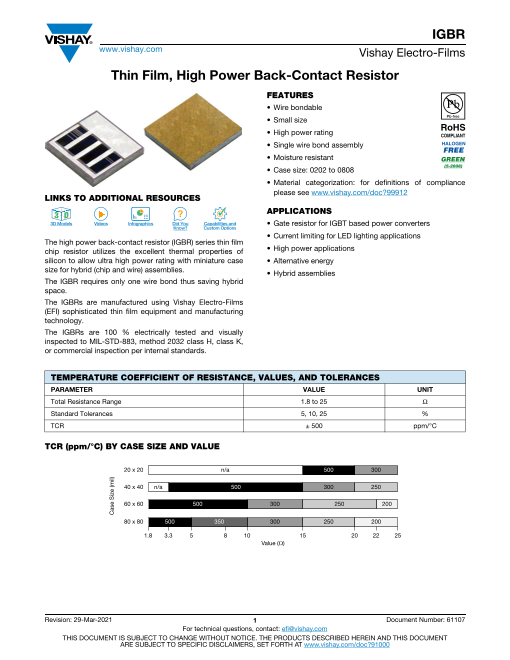


Thin Film, High Power Back-Contact Resistor
このカタログについて
| ドキュメント名 | Vishay Electro-Films IGBR |
|---|---|
| ドキュメント種別 | 製品カタログ |
| ファイルサイズ | 138.8Kb |
| 取り扱い企業 | マウザー・エレクトロニクス (この企業の取り扱いカタログ一覧) |
この企業の関連カタログ


このカタログの内容
Page1
IGBR
www.vishay.com Vishay Electro-Films
Thin Film, High Power Back-Contact Resistor
FEATURES
• Wire bondable
• Small size
• High power rating
• Single wire bond assembly
• Moisture resistant
• Case size: 0202 to 0808
• Material categorization: for definitions of complianc e
please see www.vishay.com/doc?99912
LINKS TO ADDITIONAL RESOURCES
3D 3D APPLICATIONS
3D Models Videos Infographics Did You Capabilities and • Gate resistor for IGBT based power converters
Know? Custom Options
• Current limiting for LED lighting applications
The high power back-contact resistor (IGBR) series thin film
chip resistor utilizes the excellent thermal properties o f • High power applications
silicon to allow ultra high power rating with miniature case • Alternative energy
size for hybrid (chip and wire) assemblies. • Hybrid assemblies
The IGBR requires only one wire bond thus saving hybri d
space.
The IGBRs are manufactured using Vishay Electro-Films
(EFI) sophisticated thin film equipment and manufacturing
technology.
The IGBRs are 100 % electrically tested and visually
inspected to MIL-STD-883, method 2032 class H, class K,
or commercial inspection per internal standards.
TEMPERATURE COEFFICIENT OF RESISTANCE, VALUES, AND TOLERANCES
PARAMETER VALUE UNIT
Total Resistance Range 1.8 to 25 Ω
Standard Tolerances 5, 10, 25 %
TCR ± 500 ppm/°C
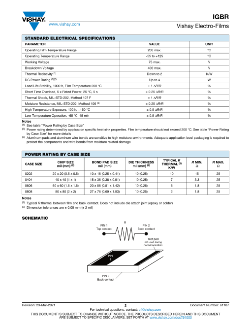
TCR (ppm/°C) BY CASE SIZE AND VALUE
20 x 20 n/a 500 300
40 x 40 n/a 500 300 250
60 x 60 500 300 250 200
80 x 80 500 350 300 250 200
1.8 3.3 5 8 10 15 20 22 25
Value ()
Revision: 29-Mar-2021 1 Document Number: 61107
For technical questions, contact: efi@vishay.com
THIS DOCUMENT IS SUBJECT TO CHANGE WITHOUT NOTICE. THE PRODUCTS DESCRIBED HEREIN AND THIS DOCUMENT
ARE SUBJECT TO SPECIFIC DISCLAIMERS, SET FORTH AT www.vishay.com/doc?91000
Case Size (mil)
Page2
IGBR
www.vishay.com Vishay Electro-Films
STANDARD ELECTRICAL SPECIFICATIONS
PARAMETER VALUE UNIT
Operating Film Temperature Range 200 max. °C
Operating Temperature Range -55 to +125 °C
Working Voltage 75 max. V
Breakdown Voltage 400 max. V
Thermal Resistivity (1) Down to 2 K/W
DC Power Rating (1)(2) Up to 4 W
Load Life Stability, 1000 h, Film Temperature 200 °C ± 1 ΔR/R %
Short Time Overload, 5 x Rated Power, 25 °C, 5 s ± 0.25 ΔR/R %
Thermal Shock, MIL-STD-202, Method 107 F ± 1 ΔR/R %
Moisture Resistance, MIL-STD-202, Method 106 (3) ± 0.25 ΔR/R %
High Temperature Exposure, 100 h, +150 °C ± 0.5 ΔR/R %
Low Temperature Operation, -65 °C, 45 min ± 0.5 ΔR/R %
Notes
(1) See table “Power Rating by Case Size”
(2) Power rating determined by application specific heat sink properties. Film temperature should not exceed 200 °C. See table “Power Rating
by Case Size” for more details
(3) Aluminum pads and aluminum wire bonds are sensitive to high moisture environments. Adequate application level packaging is required t o
protect the components and wire bonds from moisture related damage
POWER RATING BY CASE SIZE
CASE SIZE CHIP SIZE BOND PAD SIZE DIE THICKNESS TYPICAL R
THERMAL (1) R MIN. R MAX.
mil (mm) (2) mil (mm) mil (mm) (2)
K/W Ω Ω
0202 20 x 20 (0.5 x 0.5) 10 x 16 (0.25 x 0.41) 10 (0.25) 10 15 25
0404 40 x 40 (1 x 1) 15 x 36 (0.38 x 0.91) 10 (0.25) 7 3.3 25
0606 60 x 60 (1.5 x 1.5) 20 x 56 (0.51 x 1.42) 10 (0.25) 5 1.8 25
0808 80 x 80 (2 x 2) 27 x 76 (0.69 x 1.93) 10 (0.25) 2 1.8 25
Notes
(1) Typical R thermal between film and back contact. Does not include die attach joint (epoxy or solder)
(2) Dimension tolerances are ± 0.05 mm (± 2 mil)
SCHEMATIC
R
PIN 1 PIN 2
Top contact Back contact
Test pad
not used during
normal operation
PIN
1
PIN 2
Back contact
Revision: 29-Mar-2021 2 Document Number: 61107
For technical questions, contact: efi@vishay.com
THIS DOCUMENT IS SUBJECT TO CHANGE WITHOUT NOTICE. THE PRODUCTS DESCRIBED HEREIN AND THIS DOCUMENT
ARE SUBJECT TO SPECIFIC DISCLAIMERS, SET FORTH AT www.vishay.com/doc?91000
Page3
IGBR
www.vishay.com Vishay Electro-Films
MATERIAL SPECIFICATIONS
PARAMETER
Chip Substrate Material Oxidized silicon, 10 kÅ minimum SiO2
Film Material Tantalum Nitride
Case Size See table “Power Rating by Case Size”
Passivation None
Number of Pads 1
Top Terminations Suitable for Heavy Gage Aluminum Wire-Bonding Al (2.5 μm min.)
P = TiW (500 Å to 1000 Å)
Pd (2000 Å to 3000 Å)
Au (3000 Å to 5000 Å)
N = TiW (500 Å to 1000 Å)
Back Termination Ni (6000 Å to 7000 Å)
(for epoxy, lead (Pb)-free solder or silver compression assembly) Au (3000 Å to 5000 Å)
T = TiW (500 Å to 1000 Å)
Au (1000 Å to 3000 Å)
Ni (40 μ" minimum)
Au (40 μ" minimum)
MATERIAL SPECIFICATIONS
VERSION A (20 x 20)
IGBRA - 15 Ω to 25 Ω
VERSION B (40 x 40)
IGBRB - 3.3 Ω to 12.9 Ω IGBRB - 13 Ω to 25 Ω
Revision: 29-Mar-2021 3 Document Number: 61107
For technical questions, contact: efi@vishay.com
THIS DOCUMENT IS SUBJECT TO CHANGE WITHOUT NOTICE. THE PRODUCTS DESCRIBED HEREIN AND THIS DOCUMENT
ARE SUBJECT TO SPECIFIC DISCLAIMERS, SET FORTH AT www.vishay.com/doc?91000
Page4
IGBR
www.vishay.com Vishay Electro-Films
MATERIAL SPECIFICATIONS
VERSION C (60 x 60)
IGBRC - 1.8 Ω to 2.9 Ω IGBRC - 3 Ω to 5.5 Ω IGBRC - 5.6 Ω to 15.90 Ω IGBRC - 16 Ω to 25 Ω
VERSION D (80 x 80)
IGBRD - 1.8 Ω to 5.5 Ω IGBRD - 5.6 Ω to 14.9 Ω IGBRD - 15 Ω to 24.9 Ω
GLOBAL PART NUMBER INFORMATION
Global Part Number: IGBRB3000CJOPCST
Global Part Number Description: IGBR 1 mm 3 Ω 5 % 300 ppm/°C PD Commercial Tape
I G B R B 3 0 0 0 C J O P C S T
RESISTANCE RESISTANCE TOL.
MODEL SIZE MULTIPLIER CODE TCR BACKSIDE VISUAL PACKAGING
(Ω) CODE (%) (ppm/°C) TERMINATION CLASS CODE
IGBR A = 20 x 20 First 4 digits C = 0.001 J = 5 J = ± 500 P = TiW / Pd / Au C = commercial WS =
B = 40 x 40 are significant B = 0.01 K = 10 W = ± 350 N = TiW / Ni / Au H = class H waffle pack
High C = 60 x 60 figures of A = 0.1 M = 20 O = ± 300 T = TiW / Au/ K = class K 100 min., 1 mult.
power D = 80 x 80 resistance L = 25 M = ± 250 Ni/Au (1) ST = diced
back- on tape
contact
resistor
Note
(1) See “Material Specifications” table for metal thickness
Revision: 29-Mar-2021 4 Document Number: 61107
For technical questions, contact: efi@vishay.com
THIS DOCUMENT IS SUBJECT TO CHANGE WITHOUT NOTICE. THE PRODUCTS DESCRIBED HEREIN AND THIS DOCUMENT
ARE SUBJECT TO SPECIFIC DISCLAIMERS, SET FORTH AT www.vishay.com/doc?91000
Page5
Legal Disclaimer Notice
www.vishay.com Vishay
Disclaimer
ALL PRODUCT, PRODUCT SPECIFICATIONS AND DATA ARE SUBJECT TO CHANGE WITHOUT NOTICE TO IMPROV E
RELIABILITY, FUNCTION OR DESIGN OR OTHERWISE.
Vishay Intertechnology, Inc., its affiliates, agents, and employees, and all persons acting on its or their behalf (collectively ,
“Vishay”), disclaim any and all liability for any errors, inaccuracies or incompleteness contained in any datasheet or in any other
disclosure relating to any product.
Vishay makes no warranty, representation or guarantee regarding the suitability of the products for any particular purpose o r
the continuing production of any product. To the maximum extent permitted by applicable law, Vishay disclaims (i) any and all
liability arising out of the application or use of any product, (ii) any and all liability, including without limitation special,
consequential or incidental damages, and (iii) any and all implied warranties, including warranties of fitness for particular
purpose, non-infringement and merchantability.
Statements regarding the suitability of products for certain types of applications are based on Vishay's knowledge of typical
requirements that are often placed on Vishay products in generic applications. Such statements are not binding statement s
about the suitability of products for a particular application. It is the customer's responsibility to validate that a particular produc t
with the properties described in the product specification is suitable for use in a particular application. Parameters provided in
datasheets and / or specifications may vary in different applications and performance may vary over time. All operatin g
parameters, including typical parameters, must be validated for each customer application by the customer's technical experts.
Product specifications do not expand or otherwise modify Vishay's terms and conditions of purchase, including but not limited
to the warranty expressed therein.
Hyperlinks included in this datasheet may direct users to third-party websites. These links are provided as a convenience and
for informational purposes only. Inclusion of these hyperlinks does not constitute an endorsement or an approval by Vishay of
any of the products, services or opinions of the corporation, organization or individual associated with the third-party website .
Vishay disclaims any and all liability and bears no responsibility for the accuracy, legality or content of the third-party website
or for that of subsequent links.
Except as expressly indicated in writing, Vishay products are not designed for use in medical, life-saving, or life-sustainin g
applications or for any other application in which the failure of the Vishay product could result in personal injury or death.
Customers using or selling Vishay products not expressly indicated for use in such applications do so at their own risk. Please
contact authorized Vishay personnel to obtain written terms and conditions regarding products designed for such applications.
No license, express or implied, by estoppel or otherwise, to any intellectual property rights is granted by this document or by
any conduct of Vishay. Product names and markings noted herein may be trademarks of their respective owners.
© 2022 VISHAY INTERTECHNOLOGY, INC. ALL RIGHTS RESERVED
Revision: 01-Jan-2022 1 Document Number: 91000