


High Accuracy Ambient Light Sensor With I2C Interface
このカタログについて
| ドキュメント名 | Vishay Semiconductors VEML6031X00 |
|---|---|
| ドキュメント種別 | 製品カタログ |
| ファイルサイズ | 239.7Kb |
| 取り扱い企業 | マウザー・エレクトロニクス (この企業の取り扱いカタログ一覧) |
この企業の関連カタログ


このカタログの内容
Page1
VEML6031X00
www.vishay.com Vishay Semiconductors
High Accuracy Ambient Light Sensor With I2C Interface
FEATURES
• Package type: surface-mount
• Dimensions (L x W x H in mm): 2.67 x 2.45 x 0.6
• AEC-Q100 qualified
• Integrated modules: ambient light sensor (ALS)
• Supply voltage range VDD: 2.5 V to 3.6 V
• Communication via I2C interface
• I2C bus H-level range: 1.7 V to 3.6 V
• Floor life: 4 weeks, MSL 2a, according to
J-STD-020
LINKS TO ADDITIONAL RESOURCES • Low shut down current consumption:
typ. 0.5 μA
3D 3D • Material categorization: for definitions of complianc e
Design Tools Related 3D Models Application
Documents Notes please see www.vishay.com/doc?99912
DESCRIPTION AMBIENT LIGHT FUNCTION
VEML6031X00 is a high accuracy ambient light digital 16-bit • FiltronTM technology adaption: close to real human eye
resolution sensor in a miniature opaque 2.67 mm x 2.45 mm response
package. It includes a high sensitive photodiode, a low • Typical ALS output tolerance of ≤ 10 % under differen t
noise amplifier, a 16-bit A/D converter and supports a n light sources
easy to use I2C bus communication interface and additional
interrupt feature. • 16-bit dynamic range for ambient light detection from
0 lx to about 228 klx with resolution down to 0.0034 lx/ct,
The ambient light result is as digital value available. supports low transmittance (dark) lens design
APPLICATIONS • Excellent temperature compensation
Ambient light sensor in automotive for • High dynamic detection resolution
• Display backlight controls
• Infotainment systems
• Rear view mirror dimming
• Interior lighting control systems
• Head-up displays
PRODUCT SUMMARY
OPERATING I2C BUS
VOLTAGE VOLTAGE AMBIENT LIGHT AMBIENT LIGHT ADC RESOLUTION
PART NUMBER RANGE RANGE RANGE RESOLUTION OUTPUT
CODE PROXIMITY /
(V) (V) (lx) (lx) AMBIENT LIGHT
VEML6031X00 2.5 to 3.6 1.7 to 3.6 0 to 228 000 0.0034 16 bit, I2C - / 16 bit
ORDERING INFORMATION
ORDERING CODE PACKAGING VOLUME (1) REMARKS
VEML6031X00 Tape and reel MOQ: 3000 2.67 mm x 2.45 mm x 0.6 mm
VEML6031X00-GS15 Tape and reel MOQ: 10 000 2.67 mm x 2.45 mm x 0.6 mm
VEML60311X00 Tape and reel MOQ: 3000 2.67 mm x 2.45 mm x 0.6 mm
VEML60311X00-GS15 Tape and reel MOQ: 10 000 2.67 mm x 2.45 mm x 0.6 mm
Note
(1) MOQ: minimum order quantity
Rev. 1.2, 15-Oct-2021 1 Document Number: 80007
For technical questions, contact: sensorstechsupport@vishay.com
THIS DOCUMENT IS SUBJECT TO CHANGE WITHOUT NOTICE. THE PRODUCTS DESCRIBED HEREIN AND THIS DOCUMENT
ARE SUBJECT TO SPECIFIC DISCLAIMERS, SET FORTH AT www.vishay.com/doc?91000
Page2
VEML6031X00
www.vishay.com Vishay Semiconductors
SLAVE ADDRESS OPTIONS
ORDERING CODE SLAVE ADDRESS (7 bit)
VEML6031X00 0x29
VEML60311X00 0x10
ABSOLUTE MAXIMUM RATINGS (Tamb = 25 °C, unless otherwise specified)
PARAMETER TEST CONDITION SYMBOL MIN. MAX. UNIT
Supply voltage VDD 0 3.6 V
Operation temperature range Tamb -40 +110 °C
Storage temperature range Tstg -40 +110 °C
Total power dissipation Tamb ≤ 25 °C Ptot - 50 mW
Junction temperature Tj - 110 °C
BASIC CHARACTERISTICS (Tamb = 25 °C, unless otherwise specified)
PARAMETER TEST CONDITION SYMBOL MIN. TYP. MAX. UNIT
Supply voltage VDD 2.5 3.3 3.6 V
VDD = VBUS - 0.5 -
Shut down current (1) VDD = VBUS = 3.0 V Isd - - 1.2 μA
VDD is 3.6 V and VBUS = 1.7 V - 3.1 -
Operation mode current VDD is 3.3 V IDD - 280 - μA
I2C clock rate range fSCL 10 - 400 kHz
I2C bus input H-level range VBUS is 3.3 V Vih 0.7 x VDD - 3.6 V
I2C bus input L-level range VBUS is 3.3 V Vil -0.3 - 0.2 x VDD V
Digital current out (low, current sink) Iol 3 - - mA
Digital resolution (LSB count) (2) With ALS_GAIN = x 2, ALS_IT = 400 ms,
PD_DIV4 = 4/4 PD - 0.0034 - lx/step
Detectable maximum illuminance With ALS_GAIN = x 0.5, ALS_IT = 6.25 ms,
PD_DIV4 = 1/4 PD EV max. - 228 000 - lx
ALS dark offset (1) With ALS_GAIN = x 2, IT = 200 ms,
PD_DIV4 = 4/4 PD - 4 - step
IR dark offset (1) With ALS_GAIN = x 2, IT = 200 ms,
PD_DIV4 = 4/4 PD - 4 - step
Notes
(1) Light conditions: dark
(2) Light conditions: EV = 100 lx with 4300K white LED
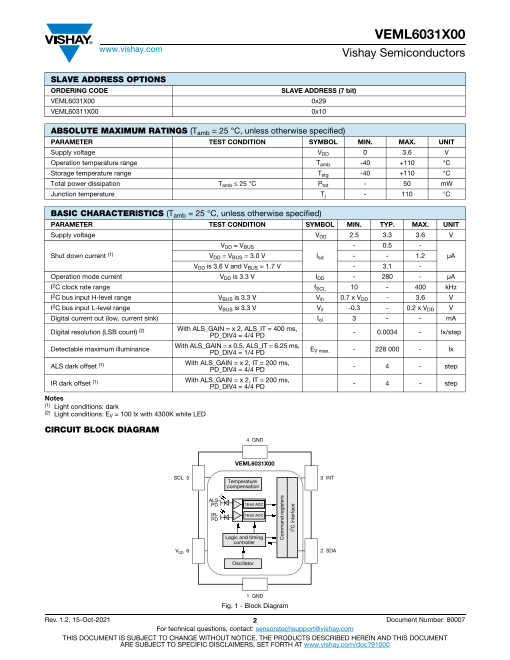
CIRCUIT BLOCK DIAGRAM
4 GND
VEML6031X00
SCL 5 3 INT
Temperature
compensation
ALS-
PD 16-bit ADC
IR- 16-bit ADC
PD
Logic and timing
controller
VDD 6 2 SDA
Oscillator
1 GND
Fig. 1 - Block Diagram
Rev. 1.2, 15-Oct-2021 2 Document Number: 80007
For technical questions, contact: sensorstechsupport@vishay.com
THIS DOCUMENT IS SUBJECT TO CHANGE WITHOUT NOTICE. THE PRODUCTS DESCRIBED HEREIN AND THIS DOCUMENT
ARE SUBJECT TO SPECIFIC DISCLAIMERS, SET FORTH AT www.vishay.com/doc?91000
Command registers
I2C interface
Page3
VEML6031X00
www.vishay.com Vishay Semiconductors
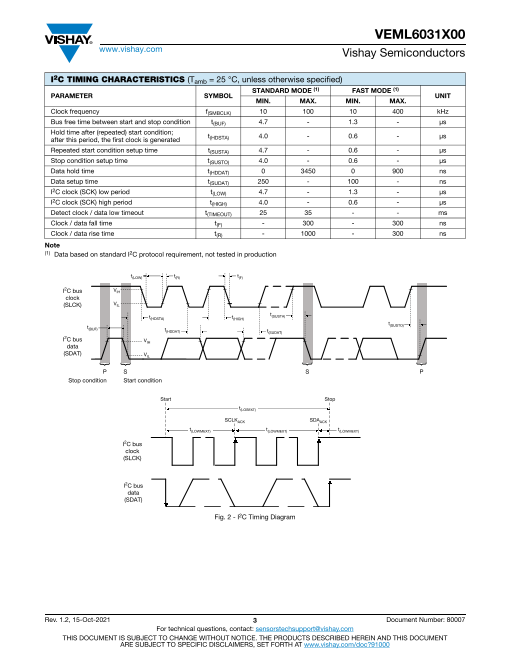
I2C TIMING CHARACTERISTICS (Tamb = 25 °C, unless otherwise specified)
STANDARD MODE (1) FAST MODE (1)
PARAMETER SYMBOL UNIT
MIN. MAX. MIN. MAX.
Clock frequency f(SMBCLK) 10 100 10 400 kHz
Bus free time between start and stop condition t(BUF) 4.7 - 1.3 - μs
Hold time after (repeated) start condition;
after this period, the first clock is generated t(HDSTA) 4.0 - 0.6 - μs
Repeated start condition setup time t(SUSTA) 4.7 - 0.6 - μs
Stop condition setup time t(SUSTO) 4.0 - 0.6 - μs
Data hold time t(HDDAT) 0 3450 0 900 ns
Data setup time t(SUDAT) 250 - 100 - ns
I2C clock (SCK) low period t(LOW) 4.7 - 1.3 - μs
I2C clock (SCK) high period t(HIGH) 4.0 - 0.6 - μs
Detect clock / data low timeout t(TIMEOUT) 25 35 - - ms
Clock / data fall time t(F) - 300 - 300 ns
Clock / data rise time t(R) - 1000 - 300 ns
Note
(1) Data based on standard I2C protocol requirement, not tested in production
t(LOW) t(R) t(F)
I2C bus VIH
clock
(SLCK) VIL
t t t(SUSTA)
(HDSTA) (HIGH)
t
t (SUSTO)
(BUF) t(HDDAT) t(SUDAT)
I2C bus VIH
data
(SDAT) VIL
P S S P
Stop condition Start condition
Start Stop
t(LOSEXT)
SCLKACK SDAACK
t(LOWMEXT) t(LOWMEXT) t(LOWMEXT)
I2C bus
clock
(SLCK)
I2C bus
data
(SDAT)
Fig. 2 - I2C Timing Diagram
Rev. 1.2, 15-Oct-2021 3 Document Number: 80007
For technical questions, contact: sensorstechsupport@vishay.com
THIS DOCUMENT IS SUBJECT TO CHANGE WITHOUT NOTICE. THE PRODUCTS DESCRIBED HEREIN AND THIS DOCUMENT
ARE SUBJECT TO SPECIFIC DISCLAIMERS, SET FORTH AT www.vishay.com/doc?91000
{
{
{
{
Page4
VEML6031X00
www.vishay.com Vishay Semiconductors
PARAMETER TIMING INFORMATION
I2C bus
clock
(SCLK)
I2C bus
data SA7 SA6 SA5 SA4 SA3 SA2 SA1 W SA7 SA6 SA5 SA4 SA3 SA2 SA1 SA0
(SDAT)
Start by ACK by ACK by
master slave slave
I2C bus slave address byte Command code
I2C bus
clock
(SCLK)
I2C bus
data SA7 SA6 SA5 SA4 SA3 SA2 SA1 SA0
(SDAT)
ACK by Stop by
slave master
Data byte
Fig. 3 - I2C Bus Timing for Sending Word Command Format
I2C bus
clock
(SCLK)
I2C bus
data SA7 SA6 SA5 SA4 SA3 SA2 SA1 W SA7 SA6 SA5 SA4 SA3 SA2 SA1 SA0
(SDAT)
Start by ACK by ACK by
master slave slave
I2C bus slave address byte Command code
I2C bus
clock
(SCLK)
I2C bus
data SA7 SA6 SA5 SA4 SA3 SA2 SA1 R SA7 SA6 SA5 SA4 SA3 SA2 SA1 SA0
(SDAT)
Start by ACK by NACK by Stop by
master slave master master
I2C bus slave address byte Data byte
Fig. 4 - I2C Bus Timing for Receive Word Command Format
Rev. 1.2, 15-Oct-2021 4 Document Number: 80007
For technical questions, contact: sensorstechsupport@vishay.com
THIS DOCUMENT IS SUBJECT TO CHANGE WITHOUT NOTICE. THE PRODUCTS DESCRIBED HEREIN AND THIS DOCUMENT
ARE SUBJECT TO SPECIFIC DISCLAIMERS, SET FORTH AT www.vishay.com/doc?91000
Page5
VEML6031X00
www.vishay.com Vishay Semiconductors
BASIC CHARACTERISTICS (Tamb = 25 °C, unless otherwise specified)
Axis Title Axis Title
1.2 10000 1.2 10000
1.0 VEML6031X00 1.0
0.8 1000 0.8 1000
0.6 0.6
V(λ)
0.4 100 0.4 100
0.2 0.2
0 10 0 10
400 500 600 700 800 900 1000 400 500 600 700 800 900 1000
λ - Wavelength (nm) λ - Wavelength (nm)
Fig. 5 - Spectral Response Fig. 6 - IR Channel Response
ALS sensitivity spectrum close to human eye photopic curve V(λ).
0° 20°
10000
1.0
0.9 40°
0.8
0.7
60°
0.6
80°
0.5 0.4 0.3 0.2 0.1 0
2nd line
Fig. 7 - Relative Sensitivity vs. Angular Displacement
Rev. 1.2, 15-Oct-2021 5 Document Number: 80007
For technical questions, contact: sensorstechsupport@vishay.com
THIS DOCUMENT IS SUBJECT TO CHANGE WITHOUT NOTICE. THE PRODUCTS DESCRIBED HEREIN AND THIS DOCUMENT
ARE SUBJECT TO SPECIFIC DISCLAIMERS, SET FORTH AT www.vishay.com/doc?91000
2nd line 2nd line
Srel - Relative Sensitivity Normalized Responsivity
- Angular Displacement 1st line
2nd line 2nd line
2nd line
Normalized Responsivity
1st line
2nd line
Page6
VEML6031X00
www.vishay.com Vishay Semiconductors
APPLICATION INFORMATION
Special care must be taken into consideration when handling the VEML6031X00. VEML6031X00 is sensitive to dust and
scratches, proper optical device handling procedures are recommended.
The optical surface of the device must be kept clean for optimal performance in both prototyping with the device and mass
production manufacturing procedures. Tweezers with plastic or rubber contact surfaces are recommended to avoid scratches
on the optical surface. Avoid manipulation with metal tools when possible. The optical surface must be kept clean of fingerprints,
dust, and other optical-inhibiting contaminants.
If the device optical surface requires cleaning, the use of isopropyl alcohol is recommended. A few gentle brushes with a sof t
swab are appropriate. Avoid potentially abrasive cleaning and manipulating tools and excessive force that can scratch th e
optical surface.
If the VEML6031X00 performs less than optimally, inspect the optical surface for dirt, scratches, or other optical artifacts.
VEML6031X00 is a cost effective solution of ambient light sensor with I2C bus interface. The standard serial digital interface is
easy to access “Ambient Light Signal” without complex calculation and programming by external controller. Beside the digita l
output also a flexible programmable interrupt pin is available.
1. Application Circuit
1.7 V to 3.6 V
R1 R2 R3
GND (1)
2.5 V to 3.6 V R4
C1 C2 VDD (6)
10R Host
10 µF 100 nF VEML6031X00 Micro Controller
SDA (2) I2C bus data SDA
SCL (5) I2C bus clock SCL
C1 and R4
are optional GND (4) INT (3) GPIO (interrupt)
for a noisy
supply
Fig. 8 - Application Circuit
(x) = Pin Number
Notes
• The interrupt pin is an open drain output. Proposed values for the pull-up resistors should be > 1 kΩ, e.g. 2.2 kΩ to 4.7 kΩ for the R1 and
R2 (at SDA and SCL) and 10 kΩ to 100 kΩ for R3 (at interrupt).
Normally just one decoupling capacitor is needed. This should be ≥ 100 nF and placed close to the VDD pin.
For detailed description about set-up and use of the interrupt as well as more application related information see AN: “Designing
VEML6031X00 into an Application”
Rev. 1.2, 15-Oct-2021 6 Document Number: 80007
For technical questions, contact: sensorstechsupport@vishay.com
THIS DOCUMENT IS SUBJECT TO CHANGE WITHOUT NOTICE. THE PRODUCTS DESCRIBED HEREIN AND THIS DOCUMENT
ARE SUBJECT TO SPECIFIC DISCLAIMERS, SET FORTH AT www.vishay.com/doc?91000
Page7
VEML6031X00
www.vishay.com Vishay Semiconductors
2. I2C Interface
The VEML6031X00 has eighteen register addresses responsible for operation control, parameter setup and result buffering .
All registers are accessible via I2C communication. Fig. 9 shows the basic I2C communication with VEML6031X00.
The built in I2C interface is compatible with I2C modes “standard” and “fast”: 10 kHz to 400 kHz.
Please refer to the I2C specification from NXP for details.
Send byte Block write byte mode
1 7 1 1 8 1 8 1 8 1 8 1
S Slave address Wr A Command code A Data byte A Data byte Data byte
(address = M) (address = M) (address = M + 1) A (address = M + 2) A
8 1 8 1 1
Data byte A Data byte
(address = M + 3) (address = M + N) A P
Receive byte Block read byte mode
1 7 1 1 8 1 1 7 1 1 8 1 8 1
S Slave address Wr A Command code Slave Data byte
(address = M) A Sr address R A (address = M) A Data byte
(address = M + 1) A
8 1 8 1 1
Data byte A Data byte
(address = M + 2) (address = M + N) N P
S = start condition Host action
P = stop condition
A = acknowledge VEML6031X00 response
Sr = reapeated start condition
Fig. 9 - Send Byte / Receive Byte Protocol
Device Address Register Addresses
The VEML6031X00 is available in two different The VEML6031X00 has eighteen registers, accessible
pre-configured slave addresses. through there respective 8-bit command codes.
For one version the predefined 7 bit I2C bus address is set The registers are 0x00 to 0x17 (0x02 and 0x03, 0x08 to 0x0F
to 0101001 = 0x29. The least significant bit (LSB) defines and 0x16 are not defined / reserved). Note that due to the
read or write mode. Accordingly the bus address is set to location of the two shutdown bits (SD and ALS_IR_SD), on e
0101 0010 = 0x52 for write and 0101 0011 = 0x53 for read. in register 0x00 and the other in 0x01, it is necessary to
The second version comes with predefined 7 bit I2C bus always write to both registers at once when configuring th e
address of 0010000 = 0x10, so, here the write address i s device.
0010 0000 = 0x20 for write and 0010 0001 = 0x21 for read.
Auto-Memorization
The VEML6031X00 stores the last measured ambient data
before the device is shutdown, keeping the data accessible.
When VEML6031X00 is in shutdown mode, the host can
freely read this data via read command directly.
Rev. 1.2, 15-Oct-2021 7 Document Number: 80007
For technical questions, contact: sensorstechsupport@vishay.com
THIS DOCUMENT IS SUBJECT TO CHANGE WITHOUT NOTICE. THE PRODUCTS DESCRIBED HEREIN AND THIS DOCUMENT
ARE SUBJECT TO SPECIFIC DISCLAIMERS, SET FORTH AT www.vishay.com/doc?91000
Page8
VEML6031X00
www.vishay.com Vishay Semiconductors
COMMAND REGISTER FORMAT
COMMAND CODE REGISTER NAME BIT DEFAULT VALUE FUNCTION / DESCRIPTION R / W
0x00 ALS_CONF 0 0 : 7 0x01 ALS integration time, measurement mode, shutdown R/W
0x01 ALS_CONF 1 0 : 7 0x00 ALS and IR shutdown, ALS gain, interrupt persistance R/W
0x04 ALS_WH_L 0 : 7 0x00 ALS high threshold window setting (LSB) R/W
0x05 ALS_WH_H 0 : 7 0x00 ALS high threshold window setting (MSB) R/W
0x06 ALS_WL_L 0 : 7 0x00 ALS low threshold window setting (LSB) R/W
0x07 ALS_WL_H 0 : 7 0x00 ALS low threshold window setting (MSB) R/W
0x10 ALS_DATA_L 0 : 7 0x00 Low byte of 16-bit ALS result DATA R
0x11 ALS_DATA_H 0 : 7 0x00 High byte of 16-bit ALS result DATA R
0x12 IR_DATA_L 0 : 7 0x00 Low byte of 16-bit IR result DATA R
0x13 IR_DATA_H 0 : 7 0x00 High byte of 16-bit IR result DATA R
0x14 ID_L 0 : 7 0x01 ID code R
0x15 ID_H 0 : 7 0x00 Package and version code R
0x17 ALS_INT 0 : 7 0x00 ALS INT trigger event R
Notes
• Command code 0x00 default value is 0x01 = device is shutdown
• Command 0x00 and command 0x01 must be executed together, they cannot be executed independently
TABLE 1 - REGISTER: ALS_CONF_0 - 0x00
REGISTER NAME BIT FUNCTION / DESCRIPTION R / W
Reserved 7 Must be set to “0” R / W
ALS integration time setting
000 = 3.125 ms
001 = 6.25 ms
010 = 12.5 ms
ALS_IT 6 : 4 011 = 25 ms R / W
100 = 50 ms
101 = 100 ms
110 = 200 ms
111 = 400 ms
Active force mode enable setting
0 = AF disable
ALS_AF 3 1 = AF enable R / W
Once enabled, a single measurement can be triggered with the “ALS_TRIG” bit
ALS active force trigger setting
0 = no active force mode trigger
ALS_TRIG 2 R / W
1 = trigger active force mode
This bit resets to “0” automatically after every trigger
ALS interrupt setting
ALS_INT_EN 1 0 = interrupt disable R / W
1 = interrupt enable
Band gap and LDO shutdown setting
SD 0 0 = band gap and LDO on R / W
1 = band gap and LDO shutdown (default)
Note
• Command code 0x00 default value is 0x01 = device is shutdown
Rev. 1.2, 15-Oct-2021 8 Document Number: 80007
For technical questions, contact: sensorstechsupport@vishay.com
THIS DOCUMENT IS SUBJECT TO CHANGE WITHOUT NOTICE. THE PRODUCTS DESCRIBED HEREIN AND THIS DOCUMENT
ARE SUBJECT TO SPECIFIC DISCLAIMERS, SET FORTH AT www.vishay.com/doc?91000
Page9
VEML6031X00
www.vishay.com Vishay Semiconductors
TABLE 2 - REGISTER: ALS_CONF_1 - 0x01
REGISTER NAME BIT FUNCTION / DESCRIPTION R / W
ALS and IR channel shutdown setting
ALS_IR_SD 7 0 = ALS and IR channels on R / W
1 = ALS and IR channels shutdown
Effective photodiode size ALS and IR
PD_DIV4 6 0 = 4/4 PD used R / W
1 = 1/4 PD used
Reserved 5 Reserved R / W
Gain selection
00 = ALS gain x1
ALS_GAIN 4 : 3 01 = ALS gain x2 R / W
10 = ALS gain x 0.66
11 = ALS gain x 0.5
ALS persistence protect number setting
Number of persistent measurements above threshold to trigger the interrupt
00 = 1
ALS_PERS 2 : 1 R / W
01 = 2
10 = 4
11 = 8
ALS_CAL 0 Must be set to “1” when power on ready R / W
TABLE 3 - REGISTER: ALS_WH - 0x04, 0x05
COMMAND CODE REGISTER NAME BIT FUNCTION / DESCRIPTION R / W
0x04 ALS_WH_L 7 : 0 ALS high threshold window setting (data byte low) R / W
0x05 ALS_WH_H 7 : 0 ALS high threshold window setting (data byte high) R / W
TABLE 4 - REGISTER: ALS_WL - 0x06, 0x07
COMMAND CODE REGISTER NAME BIT FUNCTION / DESCRIPTION R / W
0x06 ALS_WL_L 7 : 0 ALS low threshold window setting (data byte low) R / W
0x07 ALS_WL_H 7 : 0 ALS low threshold window setting (data byte high) R / W
TABLE 5 - REGISTER: ALS_DATA - 0x10, 0x11
COMMAND CODE REGISTER NAME BIT FUNCTION / DESCRIPTION R / W
0x10 ALS_DATA_L 7 : 0 ALS result channel (data byte low) R
0x11 ALS_DATA_H 7 : 0 ALS result channel (data byte high) R
TABLE 6 - REGISTER: IR_DATA - 0x12, 0x13
COMMAND CODE REGISTER NAME BIT FUNCTION / DESCRIPTION R / W
0x12 IR_DATA_L 7 : 0 IR result channel (data byte low) R
0x13 IR_DATA_H 7 : 0 IR result channel (data byte high) R
TABLE 7 - REGISTER: ID - 0x14, 0x15
COMMAND CODE REGISTER NAME BIT FUNCTION / DESCRIPTION R / W
0x14 ID_L 7 : 0 ID code: 0x01 R
7 : 6 Package code: 00
0x15 ID_H 5 : 4 Slave address: 00 = 0x29; 01 = 0x10 R
3 : 0 Version code: 0000 = A01
Rev. 1.2, 15-Oct-2021 9 Document Number: 80007
For technical questions, contact: sensorstechsupport@vishay.com
THIS DOCUMENT IS SUBJECT TO CHANGE WITHOUT NOTICE. THE PRODUCTS DESCRIBED HEREIN AND THIS DOCUMENT
ARE SUBJECT TO SPECIFIC DISCLAIMERS, SET FORTH AT www.vishay.com/doc?91000
Page10
VEML6031X00
www.vishay.com Vishay Semiconductors
TABLE 8 - REGISTER: ALS_INT - 0x17
REGISTER NAME BIT FUNCTION / DESCRIPTION R / W
Reserved 7 : 4 Reserved R
ALS_AF_DATA_READY 3 ALS active force mode data ready flag R
ALS_IF_L 2 ALS low threshold INT flag R
ALS_IF_H 1 ALS high threshold INT flag R
Reserved 0 Reserved R
CALCULATING THE LUX LEVEL
Command code 0x10 and 0x11 contain the results of th e Every time the integration time is halved, the resolution is
ALS measurement. This 16-bit code needs to be converted doubled but also the possible detection range is doubled.
to a decimal value to determine the corresponding lux value. The same principle is valid for the gain setting. Fo r
The calculation of the corresponding lux level is dependent ALS_GAIN = x1 it is doubled. For PD_DIV4 = 1/4 the size o f
on the programmed gain setting and the chosen integration the photodiode is just 1/4, so, also the sensitivity is just 1/4,
time. resolution and max. possible detection range is times 4, to
The component is most sensitive with ALS_GAIN = x2 , allow for higher illuminations up to about 228 klx.
PD_DIV4 = 4/4 and an integration time of 400 ms, specified
to 0.0034 lx/step.
TABLE 9 - RESOLUTION AND MAXIMUM DETECTION RANGE AT PD_DIV4 = 0 (= x 4/4)
GAIN x 2 GAIN x 1 GAIN x 0.66 GAIN x 0.5 GAIN x 2 GAIN x 1 GAIN x 0.66 GAIN x 0.5
IT (ms) TYPICAL RESOLUTION (lx/cnt) MAXIMUM POSSIBLE ILLUMINATION (lx)
400 0.0034 0.0068 0.0103 0.0136 223 446 675 891
200 0.0068 0.0136 0.0206 0.0272 446 891 1350 1783
100 0.0136 0.0272 0.0412 0.0544 891 1783 2701 3565
50 0.0272 0.0544 0.0824 0.1088 1783 3565 5402 7130
25 0.0544 0.1088 0.1648 0.2176 3565 7130 10803 14260
12.5 0.1088 0.2176 0.3297 0.4352 7130 14260 21607 28521
6.25 0.2176 0.4352 0.6594 0.8704 14260 28521 43213 57042
3.125 0.4352 0.8704 1.3188 1.7408 (-) (1) (-) (1) (-) (1) (-) (1)
TABLE 10 - RESOLUTION AND MAXIMUM DETECTION RANGE AT PD_DIV4 = 1 (= x 1/4)
GAIN x 2 GAIN x 1 GAIN x 0.66 GAIN x 0.5 GAIN x 2 GAIN x 1 GAIN x 0.66 GAIN x 0.5
IT (ms) TYPICAL RESOLUTION (lx/cnt) MAXIMUM POSSIBLE ILLUMINATION (lx)
400 0.0136 0.0272 0.0412 0.0544 891 1783 2701 3565
200 0.0272 0.0544 0.0824 0.1088 1783 3565 5402 7130
100 0.0544 0.1088 0.1648 0.2176 3565 7130 10803 14260
50 0.1088 0.2176 0.3297 0.4352 7130 14260 21607 28521
25 0.2176 0.4352 0.6594 0.8704 14260 28521 43213 57042
12.5 0.4352 0.8704 1.3188 1.7408 28521 57042 86427 114083
6.25 0.8704 1.7408 2.6376 3.4816 57042 114083 172854 228167
3.125 1.7408 3.4816 5.2752 6.9632 (-) (1) (-) (1) (-) (1) (-) (1)
Note
(1) For integration time of 3.125 ms the maximum count level is no longer 16 bit, so, half the integration time no longer leads to double the
max. lux level
Example:
If the 16-bit word of the ALS data shows: 0000 0101 1100 1000 = 1480 (dec.), the programmed ALS_GAIN = x1, PD_DIV4 = 4/4
(= x1) and ALS_IT = 100 ms, the corresponding lux level is: light level (lx) = 1480 x 0.0272 = 40.256 lx.
Rev. 1.2, 15-Oct-2021 10 Document Number: 80007
For technical questions, contact: sensorstechsupport@vishay.com
THIS DOCUMENT IS SUBJECT TO CHANGE WITHOUT NOTICE. THE PRODUCTS DESCRIBED HEREIN AND THIS DOCUMENT
ARE SUBJECT TO SPECIFIC DISCLAIMERS, SET FORTH AT www.vishay.com/doc?91000
Page11
VEML6031X00
www.vishay.com Vishay Semiconductors
PACKAGE DIMENSIONS in millimeters
0.4
0.8 chip surface 0.8 0.8
2.67 Pinning top view
Pin 4
GND
Pin 5 Pin 3
SCL INT
Pin 6 Pin 2
VDD SDA
Pin 1
Active area
0.2 GND
Pin 1 marking: Recommended footprint
exposed pad offset
0.15
(0.33)
0.79
0.54
0.85
Technical drawings
1.5
according to DIN
specification
Drawing No.: 6.550-5357.01-4 All dimensions in mm incl. burrs
Issue: 1; 14.04.2021 Not indicated tolerances ± 0.1
PIN 1 IDENTIFICATION
Pin 1 marking dotmarking on top side
elongated feature on bottom side
Rev. 1.2, 15-Oct-2021 11 Document Number: 80007
For technical questions, contact: sensorstechsupport@vishay.com
THIS DOCUMENT IS SUBJECT TO CHANGE WITHOUT NOTICE. THE PRODUCTS DESCRIBED HEREIN AND THIS DOCUMENT
ARE SUBJECT TO SPECIFIC DISCLAIMERS, SET FORTH AT www.vishay.com/doc?91000
1.2 2.45 0.2
0.1
0.2 0.6
(0.35)
0.85
1.28
0.79
1.2
Page12
VEML6031X00
www.vishay.com Vishay Semiconductors
TAPE AND REEL DIMENSIONS in millimeters
Reel size:
VEML6031: Ø 180 mm ± 2 mm = 3000 pcs.
VEML6031-GS 15: Ø 330 mm ± 2 mm = 10 000 pcs.
Reel design is representative for different types. Technical drawings
according to DIN
specification
Unreel direction
Not indicated tolerances ± 0.1
A
Label posted here
Pin 1
12
Sensor orientation A (5:1)
Ø 1.5
5.5 1.75
Drawing No.: 9.800-5148.01-4
Issue: prelminary; 16.10.19
Rev. 1.2, 15-Oct-2021 12 Document Number: 80007
For technical questions, contact: sensorstechsupport@vishay.com
THIS DOCUMENT IS SUBJECT TO CHANGE WITHOUT NOTICE. THE PRODUCTS DESCRIBED HEREIN AND THIS DOCUMENT
ARE SUBJECT TO SPECIFIC DISCLAIMERS, SET FORTH AT www.vishay.com/doc?91000
4
1.1
4 2 0.25
Page13
VEML6031X00
www.vishay.com Vishay Semiconductors
DRYPACK REFLOW SOLDER PROFILE
Devices are packed in moisture barrier bags (MBB) to Axis Title
prevent the products from moisture absorption durin g 300 10000
transportation and storage. Each bag contains a desiccant. Max. 260 °C
250 255 °C
240 °C 245 °C
FLOOR LIFE 217 °C
Floor life (time between soldering and removing from MBB) 200 1000
must not exceed the time indicated on MBB label: Max. 30 s
150
Floor life: 4 weeks
Max. 120 s Max. 100 s
Conditions: Tamb < 30 °C, RH < 60 % 100 100
Max. ramp down 6 °C/s
Moisture sensitivity level 2a, according to J-STD-020.
50 Max. ramp up 3 °C/s
DRYING
In case of moisture absorption devices should be bake d 0 10
0 50 100 150 200 250 300
before soldering. Conditions see J-STD-020 or label. 19841 Time (s)
Devices taped on reel dry using recommended conditions
192 h at 40 °C (+ 5 °C), RH < 5 %. Fig. 10 - Lead (Pb)-free Reflow Solder Profile
According to J-STD-020
Rev. 1.2, 15-Oct-2021 13 Document Number: 80007
For technical questions, contact: sensorstechsupport@vishay.com
THIS DOCUMENT IS SUBJECT TO CHANGE WITHOUT NOTICE. THE PRODUCTS DESCRIBED HEREIN AND THIS DOCUMENT
ARE SUBJECT TO SPECIFIC DISCLAIMERS, SET FORTH AT www.vishay.com/doc?91000
2nd line
Temperature (°C)
1st line
2nd line
Page14
Legal Disclaimer Notice
www.vishay.com Vishay
Disclaimer
ALL PRODUCT, PRODUCT SPECIFICATIONS AND DATA ARE SUBJECT TO CHANGE WITHOUT NOTICE TO IMPROV E
RELIABILITY, FUNCTION OR DESIGN OR OTHERWISE.
Vishay Intertechnology, Inc., its affiliates, agents, and employees, and all persons acting on its or their behalf (collectively ,
“Vishay”), disclaim any and all liability for any errors, inaccuracies or incompleteness contained in any datasheet or in any other
disclosure relating to any product.
Vishay makes no warranty, representation or guarantee regarding the suitability of the products for any particular purpose o r
the continuing production of any product. To the maximum extent permitted by applicable law, Vishay disclaims (i) any and all
liability arising out of the application or use of any product, (ii) any and all liability, including without limitation special,
consequential or incidental damages, and (iii) any and all implied warranties, including warranties of fitness for particular
purpose, non-infringement and merchantability.
Statements regarding the suitability of products for certain types of applications are based on Vishay's knowledge of typical
requirements that are often placed on Vishay products in generic applications. Such statements are not binding statement s
about the suitability of products for a particular application. It is the customer's responsibility to validate that a particular produc t
with the properties described in the product specification is suitable for use in a particular application. Parameters provided in
datasheets and / or specifications may vary in different applications and performance may vary over time. All operatin g
parameters, including typical parameters, must be validated for each customer application by the customer's technical experts.
Product specifications do not expand or otherwise modify Vishay's terms and conditions of purchase, including but not limited
to the warranty expressed therein.
Hyperlinks included in this datasheet may direct users to third-party websites. These links are provided as a convenience and
for informational purposes only. Inclusion of these hyperlinks does not constitute an endorsement or an approval by Vishay of
any of the products, services or opinions of the corporation, organization or individual associated with the third-party website .
Vishay disclaims any and all liability and bears no responsibility for the accuracy, legality or content of the third-party website
or for that of subsequent links.
Except as expressly indicated in writing, Vishay products are not designed for use in medical, life-saving, or life-sustainin g
applications or for any other application in which the failure of the Vishay product could result in personal injury or death.
Customers using or selling Vishay products not expressly indicated for use in such applications do so at their own risk. Please
contact authorized Vishay personnel to obtain written terms and conditions regarding products designed for such applications.
No license, express or implied, by estoppel or otherwise, to any intellectual property rights is granted by this document or by
any conduct of Vishay. Product names and markings noted herein may be trademarks of their respective owners.
© 2022 VISHAY INTERTECHNOLOGY, INC. ALL RIGHTS RESERVED
Revision: 01-Jan-2022 1 Document Number: 91000