


3 V to 28 V Input, 8 A, 12 A microBUCK DC/DC Converter
このカタログについて
| ドキュメント名 | Vishay Siliconix SiC437, SiC438 |
|---|---|
| ドキュメント種別 | 製品カタログ |
| ファイルサイズ | 2.3Mb |
| 取り扱い企業 | マウザー・エレクトロニクス (この企業の取り扱いカタログ一覧) |
この企業の関連カタログ


このカタログの内容
Page1
SiC437, SiC438
www.vishay.com Vishay Siliconix
3 V to 28 V Input, 8 A, 12 A
microBUCK® DC/DC Converter
FEATURES
• Versatile
- Operation from 3 V to 28 V input voltage
- Adjustable output voltage down to 0.6 V
- Scalable solution 8 A (SiC438), 12 A (SiC437),
and 24 A (SiC431)
LINKS TO ADDITIONAL RESOURCES - Output voltage tracking and sequencing with pre-bia s
start up
Simulation Evaluation Design Tools - ± 1 % output voltage accuracy at -40 °C to +125 °C
Tool Boards • Highly efficient
DESCRIPTION - 97 % peak efficiency
The SiC43x are synchronous buck regulators with
integrated high side and low side power MOSFETs. It s - 1 μA supply current at shutdown
power stage is capable of supplying 12 A (SiC437) and 8 A - 50 μA operating current not switching
(SiC438) continuous current at up to 1 MHz switching • Highly configurable
frequency. This regulator produces an adjustable output
voltage down to 0.6 V from 3 V to 28 V input rail to - Four programmable switching frequencies available:
accommodate a variety of applications, includin g 300 kHz, 500 kHz, 750 kHz, and 1 MHz
computing, consumer electronics, telecom, and industrial. - Adjustable soft start and adjustable current limit
SiC437’s and SiC438’s architecture delivers ultrafas t
transient response with minimum output capacitance and - Three modes of operation: forced continuous
tight ripple regulation at very light load. The device is conduction, power save (SiC43xB, SiC43xD), o r
internally compensated and is stable with any capacitor. No ultrasonic (SiC43xA, SiC43xC)
external ESR network is required for loop stability purposes .
The device also incorporates a power saving scheme tha t • Robust and reliable
significantly increases light load efficiency. - Cycle-by-cycle current limit
The regulator family integrates a full protection feature set, - Output overvoltage protection
including output overvoltage protection (OVP), cycle by
cycle overcurrent protection (OCP) short circuit protectio n - Output undervoltage / short circuit protection with auto
(SCP) and thermal shutdown (OTP). It also has UVLO and a retry
user programmable soft start. - Power good flag and over temperature protection
The SiC437 and SiC438 are available in lead (Pb)-free powe r
enhanced MLP-44L package in 4 mm x 4 mm dimension. • Material categorization: for definitions of complianc e
please see www.vishay.com/doc?99912
APPLICATIONS
• 5 V, 12 V, and 24 V input rail POLs
• Desktop, notebooks, server, and industrial computing
• Industrial and automation
• consumer electronics
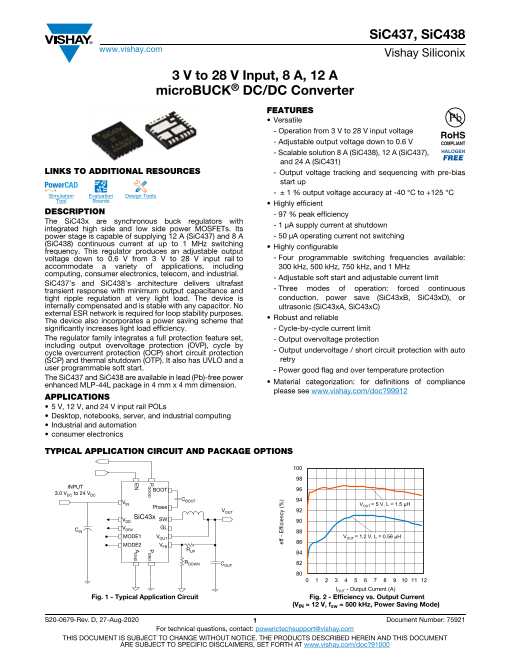
TYPICAL APPLICATION CIRCUIT AND PACKAGE OPTIONS
Axis Title
100 10000
98
INPUT BOOT 96
3.0 VDC to 24 VDC
C
V BOOT 94
IN
Phase VOUT = 5 V, L = 1.5 µH 1000
VOUT 92
V SiC43x
DD SW 90
C V
IN DRV GL
88
MODE1 VOUT VOUT = 1.2 V, L = 0.56 µH 100
MODE2 V 86
FB
RUP 84
RDOWN COUT 82
80 10
0 1 2 3 4 5 6 7 8 9 10 11 12
IOUT - Output Current (A)
Fig. 1 - Typical Application Circuit Fig. 2 - Efficiency vs. Output Current
(VIN = 12 V, fsw = 500 kHz, Power Saving Mode)
S20-0679-Rev. D, 27-Aug-2020 1 Document Number: 75921
For technical questions, contact: powerictechsupport@vishay.com
THIS DOCUMENT IS SUBJECT TO CHANGE WITHOUT NOTICE. THE PRODUCTS DESCRIBED HEREIN AND THIS DOCUMENT
ARE SUBJECT TO SPECIFIC DISCLAIMERS, SET FORTH AT www.vishay.com/doc?91000
2nd line
eff - Efficiency (%)
1st line
2nd line
PGOOD PGND
EN AGND
Page2
SiC437, SiC438
www.vishay.com Vishay Siliconix
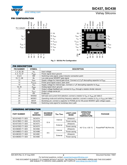
PIN CONFIGURATION
Pin 1 indicator
17 FB FB 17
V 1 16 A A 25 26
IN GND GND 16 1 V
A IN
GND VIN
VIN 2 15 VDD VDD 15 2 VIN
14 PGOOD PGOOD 14
PGND 3 13 PGND PGND 13 27 3 PGND
P
P 4 12 V GND
GND DRV VDRV 12 4 PGND
11 GL GL 11
28
GL
Fig. 3 - SiC43x Pin Configuration
PIN DESCRIPTION
PIN NUMBER SYMBOL DESCRIPTION
1, 2, 22, 26 VIN Input voltage
3, 4, 13, 27 PGND Power signal return ground
5 to 9 SW Switching node signal; output inductor connection point
10, 11, 28 GL Low side power MOSFET gate signal
12 VDRV Supply voltage for internal gate driver. Connect a 2.2 μF decoupling capacitor to PGND
14 PGOOD Power good signal output; open drain
15 VDD Supply voltage for internal logic. Connect a 1 μF decoupling capacitor to AGND
16, 25 AGND Analog signal return ground
17 FB Output voltage feedback pin; connect to VOUT through a resistor divider network.
18 VOUT Output voltage sense pin
19 EN Enable pin
20 MODE2 Soft start and current limit selection; connect a resistor to VDD or AGND per table 2
21 MODE1 Operating mode and switching frequency selection; connect a resistor to VDD or AGND per table 1
23 BOOT Bootstrap pin; connect a capacitor to PHASE pin for HS power MOSFET gate voltage supply
24 PHASE Switching node signal for bootstrap return path
ORDERING INFORMATION
PART NUMBER PART MAXIMUM V , V LIGHT LOAD OPERATING
MARKING CURRENT DD DRV MODE JUNCTION PACKAGE
TEMPERATURE
SiC437AED-T1-GE3 SiC437A Ultrasonic
Internal
SiC437BED-T1-GE3 SiC437B Power saving
12 A
SiC437CED-T1-GE3 SiC437C Ultrasonic
External
SiC437DED-T1-GE3 SiC437D Power saving
-40 °C to +125 °C PowerPAK® MLP44-24L
SiC438AED-T1-GE3 SiC438A Ultrasonic
Internal
SiC438BED-T1-GE3 SiC438B Power saving
8 A
SiC438CED-T1-GE3 SiC438C Ultrasonic
External
SiC438DED-T1-GE3 SiC438D Power saving
S20-0679-Rev. D, 27-Aug-2020 2 Document Number: 75921
For technical questions, contact: powerictechsupport@vishay.com
THIS DOCUMENT IS SUBJECT TO CHANGE WITHOUT NOTICE. THE PRODUCTS DESCRIBED HEREIN AND THIS DOCUMENT
ARE SUBJECT TO SPECIFIC DISCLAIMERS, SET FORTH AT www.vishay.com/doc?91000
SW 5 24 PHASE
SW 6 23 BOOT
SW 7 22 VIN
SW 8 21 MODE1
SW 9 20 MODE2
GL 10 19 EN
18 VOUT
18 VOUT
GL 10 19 EN
SW 9 20 MODE2
SW 8 21 MODE1
SW 7 22 VIN
SW 6 23 BOOT
SW 5 24 PHASE
Page3
SiC437, SiC438
www.vishay.com Vishay Siliconix
ABSOLUTE MAXIMUM RATINGS (TA = 25 °C, unless otherwise noted)
ELECTRICAL PARAMETER CONDITIONS LIMITS UNIT
VIN Reference to PGND -0.3 to +30
VOUT Reference to PGND -0.3 to +22
VDD / VDRV Reference to PGND -0.3 to +6
SW / PHASE Reference to PGND -0.3 to +30
SW / PHASE (AC) 100 ns;
reference to P -8 to +35
GND V
BOOT Reference to PGND -0.3 to +6
BOOT to SW -0.3 to +6
AGND to PGND -0.3 to +0.3
EN Reference to AGND -0.3 to +30
All other pins Reference to AGND -0.3 to +6
Temperature
Junction temperature TJ -40 to +150
°C
Storage temperature TSTG -65 to +150
Power Dissipation
Junction to ambient thermal impedance (RJA) 16
°C/W
Junction to case thermal impedance (RJC) 2
Maximum power dissipation Ambient temperature = 25 °C 7.75 W
ESD Protection
Human body model 4000
Electrostatic discharge protection V
Charged device model 1000
Stresses beyond those listed under “Absolute Maximum Ratings” may cause permanent damage to the device. These are stress ratings only, and functional operation
of the device at these or any other conditions beyond those indicated in the operational sections of the specifications is not implied. Exposure to absolute maximum
rating/conditions for extended periods may affect device reliability.
RECOMMENDED OPERATING CONDITIONS (all voltages referenced to GND = 0 V)
PARAMETER MIN. TYP. MAX. UNIT
Input voltage (VIN) (SiC43xA, SiC43xB) 4.5 - 28
Input voltage (VIN) (SiC43xC, SiC43xD) 3 - 28
Logic supply voltage, gate driver supply voltage (VDD, VDRV)
(SiC43xC, SiC43xD) 4.5 - 28
V
Enable (EN) 0 - 28
Input voltage (VIN), external supply on VDD / VDRV 3 - 28
Output voltage (V ) 0.6 - 0.9 x VIN
OUT and < 20 V
Temperature
Recommended ambient temperature -40 to +105
°C
Operating junction temperature -40 to +125
S20-0679-Rev. D, 27-Aug-2020 3 Document Number: 75921
For technical questions, contact: powerictechsupport@vishay.com
THIS DOCUMENT IS SUBJECT TO CHANGE WITHOUT NOTICE. THE PRODUCTS DESCRIBED HEREIN AND THIS DOCUMENT
ARE SUBJECT TO SPECIFIC DISCLAIMERS, SET FORTH AT www.vishay.com/doc?91000
Page4
SiC437, SiC438
www.vishay.com Vishay Siliconix
ELECTRICAL SPECIFICATIONS (VIN = 12 V, VEN = 5 V, TJ = -40 °C to +125 °C, unless otherwise stated)
PARAMETER SYMBOL TEST CONDITIONS MIN. TYP. MAX. UNIT
Power Supplies
VDD supply V VIN = 6 V to 28 V
DD (SiC43xA, SiC43xB) 4.75 5 5.25
V
VDD UVLO threshold, rising VDD_UVLO 3.3 3.6 3.9
VDD UVLO hysteresis VDD_UVLO_HYST - 300 - mV
Maximum VDD current IDD VIN = 6 V to 28 V 3 - - mA
V supply V VIN = 6 V to 28 V
DRV DRV (SiC43xA, SiC43xB) 4.75 5 5.25 V
Maximum VDRV current IDRV VIN = 6 V to 28 V 50 - - mA
Input current IVIN Non-switching, VFB > 0.6 V - 50 120
μA
Shutdown current IVIN_SHDN VEN = 0 V - 0.5 3
Controller and Timing
TJ = 25 °C 597 600 603
Feedback voltage VFB m/V
TJ = -40 °C to +125 °C (1) 594 600 606
VFB input bias current IFB - 2 - nA
Minimum on-time tON_MIN. - 50 65 ns
tON accuracy tON_ACCURACY -10 - 10 %
On-time range tON_RANGE 65 - 2250 ns
Ultrasonic version (SiC43xA, SiC43xC) 20 - 30
Minimum frequency, skip mode fSW_MIN. kHz
Power save version (SiC43xB, SiC43xD) 0 - -
Minimum off-time tOFF_MIN. 205 250 305 ns
Power MOSFETs (SiC437)
High side on resistance RON_HS - 10.1 -
VDRV = 5 V, TA = 25 °C m
Low side on resistance RON_LS - 3.9 -
Power MOSFETs (SiC438)
High side on resistance RON_HS - 10.1 -
VDRV = 5 V, TA = 25 °C m
Low side on resistance RON_LS - 5.5 -
Fault Protections
Over current protection
(inductor valley current) IOCL_P TJ = -10 °C to +125 °C -20 - 20
Output OVP threshold V %
OVP - 20 -
VFB with respect to 0.6 V reference
Output UVP threshold VUVP - -80 -
TOTP_RISING Rising temperature - 150 -
Over temperature protection °C
TOTP_HYST Hysteresis - 25 -
Power Good
VFB_RISING_VTH_OV VFB rising above 0.6 V reference - 20 -
Power good output threshold %
VFB_FALLING_VTH_UV VFB falling below 0.6 V reference - -10 -
Power good hysteresis VFB_HYST - 40 - mV
Power good on resistance RON_PGOOD - 7.5 15
Power good delay time tDLY_PGOOD 15 25 35 μs
EN / MODE / Ultrasonic Threshold
EN logic high level VEN_H 1.6 - -
V
EN logic low level VEN_L - - 0.4
EN pull down resistance REN - 5 - M
Switching Frequency
fsw = 300 kHz - 51 55
fsw = 500 kHz 90 100 110
MODE1 (switching frequency) RMODE1 k
fsw = 750 kHz 180 200 220
fsw = 1000 kHz 450 499 550
S20-0679-Rev. D, 27-Aug-2020 4 Document Number: 75921
For technical questions, contact: powerictechsupport@vishay.com
THIS DOCUMENT IS SUBJECT TO CHANGE WITHOUT NOTICE. THE PRODUCTS DESCRIBED HEREIN AND THIS DOCUMENT
ARE SUBJECT TO SPECIFIC DISCLAIMERS, SET FORTH AT www.vishay.com/doc?91000
Page5
SiC437, SiC438
www.vishay.com Vishay Siliconix
ELECTRICAL SPECIFICATIONS (VIN = 12 V, VEN = 5 V, TJ = -40 °C to +125 °C, unless otherwise stated)
PARAMETER SYMBOL TEST CONDITIONS MIN. TYP. MAX. UNIT
Soft Start
Connect RMODE2 between
MODE2 and A 1.8 3 4.2
GND
Soft start time tss ms
Connect RMODE2 between
MODE2 and V 3.6 6 8.4
DD
Over Current Protection - SiC437
IOCP = 18 A 450 499 550
IOCP = 14 A 180 200 220
MODE 2 (over current protection) RMODE2 k
IOCP = 9.7 A 90 100 110
IOCP = 5.4 A - 51 55
Over Current Protection - SiC438
IOCP = 12 A 450 499 550
IOCP = 9.3 A 180 200 220
MODE 2 (over current protection) RMODE2 k
IOCP = 6.5 A 90 100 110
IOCP = 3.6 A - 51 55
Note
(1) Guaranteed by design
FUNCTIONAL BLOCK DIAGRAM
VIN VOUT
V Sync
DRV Regulator rectifier
Rr
VDD UVLO BOOT
EN Enable
MODE1
PH
Over voltage Control
under voltage logic SW
SW VDRV
VOUT Ramp On time
generator
FB
R Zero GL
Reference c crossing
C PGOOD
c
Soft start
Over Over
MODE2 current temperature Power good
AGND PGND
Fig. 4 - SiC43x Functional Block Diagram
S20-0679-Rev. D, 27-Aug-2020 5 Document Number: 75921
For technical questions, contact: powerictechsupport@vishay.com
THIS DOCUMENT IS SUBJECT TO CHANGE WITHOUT NOTICE. THE PRODUCTS DESCRIBED HEREIN AND THIS DOCUMENT
ARE SUBJECT TO SPECIFIC DISCLAIMERS, SET FORTH AT www.vishay.com/doc?91000
EA
Page6
SiC437, SiC438
www.vishay.com Vishay Siliconix
OPERATIONAL DESCRIPTION
Device Overview • Slow path is the error amplifier loop which ensures the DC
The SiC43x is high efficiency synchronous buck regulators component of the output voltage follows the internal
capable of delivering up to 8 A (SiC438) and 12 A (SiC437 ) accurate reference voltage
continuous current. The device has user programmable
switching frequency of 300 kHz, 500 kHz, 750 kHz, and L VOUT
V V
1 MHz. The control scheme delivers fast transient response IN SW OUT
and minimizes the number of external components. Thank s Ramp RUP
to the internal ramp information, no high ESR output bulk or Cinj2 Rinj FB
Cinj1 Load
INPUT
virtual ESR network is required for the loop stability. This PWM COUT
Comp RDOWN
device also incorporates a power saving feature that Ripple based Error Amp
controller Ref.
enables diode emulation mode and frequency fold back as RCOMP
the load decreases. C
SiC43x COMP
SiC43x has a full set of protection and monitoring features: AGND
• Over current protection in pulse-by-pulse mode
• Output over voltage protection Fig. 5 - VM-COT Block Diagram
• Output under voltage protection with device latch All components for RAMP signal generation and erro r
• Over temperature protection with hysteresis amplifier compensation required for the control loop are
internal to the IC, see Fig. 5. In order for the device to cover
• Dedicated enable pin for easy power sequencing a wide range of VOUT operation, the internal RAMP signal
• Power good open drain output components (RX, CX, CY) are automatically selected
This device is available in MLP44-24L package to deliver depending on the VOUT voltage and switching frequency .
high power density and minimize PCB area. This method allows the RAMP amplitude to remain constan t
throughout the VOUT voltage range, achieving low jitter and
Power Stage fast transient Response. The error amplifier internal
SiC43x integrates a high performance power stage with a compensation consists of a resistor in series with a
low on resistance and gate charge, high side and lo w capacitor (RCOMP, CCOMP).
side MOSFETs. The MOSFETs are optimized to achieve up Fig. 6 demonstrates the basic operational waveforms:
to 97 % efficiency.
The input voltage (VIN) can go up to 28 V and down to as low
VRAMP
as 3 V for power conversion. For input voltages (VIN) below
4.5 V an external VDD and VDRV supply is required (SiC43xC ,
SiC43xD). For input voltages (VIN) above 4.5 V only a singl e VCOMP
input supply is required (SiC43xA, SiC43xB).
Control Mechanism
SiC43x employs an advanced voltage - mode COT control PWM
mechanism. During steady-state operation, feedback Fixed on-time
voltage (VFB) is compared with internal reference (0.6 V typ. ) Fig. 6 - VM-COT Operational Principle
and the amplified error signal (VCOMP) is generated at the Light Load Condition
internal comp node. An internally generated ramp signal an d To improve efficiency at light-load condition, SiC437,
VCOMP feed into a comparator. Once VRAMP crosses VCOMP, SiC438 provide a set of innovative implementations to
an on-time pulse is generated for a fixed time. During th e eliminate LS recirculating current and switching losses. Th e
on-time pulse, the high side MOSFET will be turned on. internal zero crossing detector monitors SW node voltage t o
Once the on-time pulse expires, the low side MOSFET will determine when inductor current starts to flow negatively. In
be turned on after a dead time period. The low side MOSFET power saving mode, as soon as inductor valley current
will stay on for a minimum duration equal to the minimum crosses zero, the device deploys diode emulation mode b y
off-time (tOFF_MIN.) and remains on until VRAMP crosses turning off low side MOSFET. If load further decreases ,
VCOMP. The cycle is then repeated. switching frequency is reduced proportional to load
Fig. 5 illustrates the basic block diagram for VM-COT condition to save switching losses while keeping output
architecture. In this architecture the following is achieved: ripple within tolerance. The switching frequency is set by th e
• The reference of a basic ripple control regulator i s controller to maintain regulation. In the standard power save
replaced with a high again error amplifier loop mode, there is no minimum switching frequency (SiC43xB,
SiC43xD). For SiC43xA, SiC43xC, the minimum switching
• This establishes two parallel voltage regulating feedbac k
paths, a fast and slow path frequency that the regulator will reduce to is > 20 kHz as the
part avoids switching frequencies in the audible range. This
• Fast path is the ripple injection which ensures rapid light load mode implementation is called ultrasonic mode.
correction of the transient perturbation
S20-0679-Rev. D, 27-Aug-2020 6 Document Number: 75921
For technical questions, contact: powerictechsupport@vishay.com
THIS DOCUMENT IS SUBJECT TO CHANGE WITHOUT NOTICE. THE PRODUCTS DESCRIBED HEREIN AND THIS DOCUMENT
ARE SUBJECT TO SPECIFIC DISCLAIMERS, SET FORTH AT www.vishay.com/doc?91000
Page7
SiC437, SiC438
www.vishay.com Vishay Siliconix
MODE SETTING, OVER CURRENT PROTECTION, SWITCHING FREQUENCY, AND SOFT START
SELECTION
The SiC437, SiC438 has a low pin count, minimal external MODE1 and MODE2, are user programmable by connectin g
components, and offers the user flexibility to choose soft a resistor from MODEx to VDD or AGND, allowing the user t o
start times, current limit settings, switching frequencies an d choose various operating modes. This is best explained in
to enable or disable the light load mode. Two MODE pins , the tables below.
TABLE 1 - MODE1 CONFIGURATION SETTINGS
OPERATION CONNECTION fSWITCH (kHz) RMODE1 (k)
300 51
500 100
Skip to AGND
750 200
1000 499
300 51
500 100
Forced CCM to VDD
750 200
1000 499
TABLE 2 - MODE2 CONFIGURATION SETTINGS
SOFT-START TIME CONNECTION ILIMIT (%) RMODE2 (k)
30 51
54 100
3 ms to AGND 78 200
100 % (18 A on SiC437)
100 % (12 A on SiC438) 499
30 51
54 100
6 ms to VDD 78 200
100 % (18 A on SiC437)
100 % (12 A on SiC438) 499
OUTPUT MONITORING AND PROTECTION FEATURES
Output Overcurrent Protection (OCP)
SiC437, SiC438 has pulse-by-pulse over current limit
control. The inductor current is monitored during low sid e
MOSFET conduction time through RDS(on) sensing. After a OCPthreshold
pre-defined blanking time, the inductor current is compare d
with an internal OCP threshold. If inductor current is highe r Iload
than OCP threshold, high side MOSFET is kept off until the Iinductor
inductor current falls below OCP threshold.
OCP is enabled immediately after VDD passes UVLO risin g
threshold.
GH
Fig. 7 - Over-Current Protection Illustration
S20-0679-Rev. D, 27-Aug-2020 7 Document Number: 75921
For technical questions, contact: powerictechsupport@vishay.com
THIS DOCUMENT IS SUBJECT TO CHANGE WITHOUT NOTICE. THE PRODUCTS DESCRIBED HEREIN AND THIS DOCUMENT
ARE SUBJECT TO SPECIFIC DISCLAIMERS, SET FORTH AT www.vishay.com/doc?91000
Page8
SiC437, SiC438
www.vishay.com Vishay Siliconix
Output Undervoltage Protection (UVP)
UVP is implemented by monitoring the FB pin. If the voltage
level at FB drops below 0.12 V for more than 25 μs, a UV P
event is recognized and both high side and low sid e
MOSFETs are turned off. After a duration equivalent to
20 soft start periods, the IC attempts to re-start. If the fault
condition still exists, the above cycle will be repeated.
UVP is active after the completion of soft start sequence.
Output Overvoltage Protection (OVP)
OVP is implemented by monitoring the FB pin. If the voltag e
level at FB rising above 0.72 V, a OVP event is recognized
and both high side and low side MOSFETs are turned off .
Normal operation is resumed once FB voltage drop below
0.68 V. Fig. 8 - Pre-Bias Start-Up
OOVP is active after VDD passes UVLO rising threshold.
Power Good
Over-Temperature Protection (OTP) SiC437, SiC438 power good is an open-drain output. Pull
OTP is implemented by monitoring the junction PGOOD pin high through a > 10 k resistor to use this signal.
temperature. If the junction temperature rises above 150 °C, Power good window is shown in the below diagram. If
a OTP event is recognized and both high side and lo w voltage on FB pin is out of this window, PGOOD signal i s
MOSFETs are turned off. After the junction temperature falls de-asserted by pulling down to AGND. To prevent fals e
below 125 °C (25 °C hysteresis), the device restarts b y triggering during transient events, PGOOD has a 25 μ s
initiating a soft start sequence. blanking time.
Sequencing of Input / Output Supplies
SiC437, SiC438 have no sequencing requirements on it s VFB_Rising_Vth_OV
(typ. = 0.72 V)
supplies or enables (VIN, VDD, V VFB_Falling_Vth_OV
DRV, EN). (typ. = 0.68 V)
Vref (0.6 V)
VFB_Falling_Vth_UV
Enable VFB (typ. = 0.54 V) VFB_Rising_Vth_UV
(typ. = 0.58 V)
The SiC437, SiC438 have an enable pin to turn the part on
and off.
Pull-high
Driving the pin high enables the device, while driving the pin PG
low disables the device.
The EN pin is internally pulled to AGND by a 5 M resistor to
Pull-low
prevent unwanted turn on due to a floating GPIO.
Fig. 9 - PGOOD Window Diagram
Pre-Bias Start-Up
In case of pre-bias startup, output is monitored through FB
pin. If the sensed voltage on FB is higher than the internal
reference ramp value, control logic prevents high side and
low side MOSFETs from switching to avoid negative outpu t
voltage spike and excessive current sinking through lo w
side MOSFET.
S20-0679-Rev. D, 27-Aug-2020 8 Document Number: 75921
For technical questions, contact: powerictechsupport@vishay.com
THIS DOCUMENT IS SUBJECT TO CHANGE WITHOUT NOTICE. THE PRODUCTS DESCRIBED HEREIN AND THIS DOCUMENT
ARE SUBJECT TO SPECIFIC DISCLAIMERS, SET FORTH AT www.vishay.com/doc?91000
Page9
SiC437, SiC438
www.vishay.com Vishay Siliconix
ELECTRICAL CHARACTERISTICS
(VIN = 12 V, VOUT = 1.2 V, fsw = 500 kHz, COUT = 47 μF x 7, CIN = 10 μF x 6, unless otherwise noted)
Axis Title Axis Title
100 10000 100 10000
VOUT = 5 V, L = 1.5 µH
98 97
96 94
94 1000 91 VOUT = 5 V, L = 1.5 µH 1000
92 88
90 85
VOUT = 1.2 V, L = 0.56 µH
88 82
86 100 79 VOUT = 1.2 V, L = 0.56 µH 100
84 76
82 73
80 10 70 10
0 1 2 3 4 5 6 7 8 9 10 11 12 0.01 0.1 1
IOUT - Output Current (A) IOUT - Output Current (A)
Fig. 10 - SiC437 Efficiency vs. Output Current Fig. 13 - SiC437 Efficiency vs. Output Current
(VIN = 12 V, fsw = 500 kHz, Full Load) (VIN = 12 V, fsw = 500 kHz, Light Load)
Axis Title Axis Title
100 10000 100 10000
98 95
96 90 VOUT = 5 V, L = 1.5 µH
85
94 VOUT = 5 V, L = 1.5 µH
1000 80 1000
92 75 VOUT = 1.2 V, L = 0.56 µH
90 70
88 VOUT = 1.2 V, L = 0.56 µH 65
86 100 60 100
55
84 50
82 45
80 10 40 10
0 1 2 3 4 5 6 7 8 9 10 11 12 0.01 0.1 1
IOUT - Output Current (A) IOUT - Output Current (A)
Fig. 11 - SiC437 Efficiency vs. Output Current Fig. 14 - SiC437 Efficiency vs. Output Current
(VIN = 12 V, fsw = 500 kHz, Ultrasonic Mode, Full Load) (VIN = 12 V, fsw = 500 kHz, Ultrasonic Mode, Light Load)
Axis Title Axis Title
100 10000 100 10000
98 97
96 94
94 1000 91 1000
92 88
VOUT = 1.2 V, L = 0.56 µH
90 VOUT = 1.2 V, L = 0.56 µH 85
88 82
86 100 79 100
84 76
82 73
80 10 70 10
0 1 2 3 4 5 6 7 8 9 10 11 12 0.01 0.1 1
IOUT - Output Current (A) IOUT - Output Current (A)
Fig. 12 - SiC437 Efficiency vs. Output Current Fig. 15 - SiC437 Efficiency vs. Output Current
(VIN = 5 V, fsw = 500 kHz, Full Load) (VIN = 5 V, fsw = 500 kHz, Light Load)
S20-0679-Rev. D, 27-Aug-2020 9 Document Number: 75921
For technical questions, contact: powerictechsupport@vishay.com
THIS DOCUMENT IS SUBJECT TO CHANGE WITHOUT NOTICE. THE PRODUCTS DESCRIBED HEREIN AND THIS DOCUMENT
ARE SUBJECT TO SPECIFIC DISCLAIMERS, SET FORTH AT www.vishay.com/doc?91000
2nd line 2nd line 2nd line
eff - Efficiency (%) eff - Efficiency (%) eff - Efficiency (%)
1st line 1st line 1st line
2nd line 2nd line 2nd line
2nd line 2nd line 2nd line
eff - Efficiency (%) eff - Efficiency (%) eff - Efficiency (%)
1st line 1st line 1st line
2nd line 2nd line 2nd line
Page10
SiC437, SiC438
www.vishay.com Vishay Siliconix
ELECTRICAL CHARACTERISTICS
(VIN = 12 V, VOUT = 1.2 V, fsw = 500 kHz, COUT = 47 μF x 7, CIN = 10 μF x 6, unless otherwise noted)
Axis Title Axis Title
100 10000 100 10000
98 VOUT = 5 V, L = 0.82 µH 97 VOUT = 5 V, L = 0.82 µH
96 94
94 1000 91 1000
92 VOUT = 3.3 V, L = 0.56 µH 88
90 85 VOUT = 3.3 V, L = 0.56 µH
88 82
86 V = 1.2 V, L = 0.36 µH 100 79 100
OUT
VOUT = 1.2 V, L = 0.36 µH
84 76
82 73
80 10 70 10
0 1 2 3 4 5 6 7 8 9 10 11 12 0.01 0.1 1
IOUT - Output Current (A) IOUT - Output Current (A)
Fig. 16 - SIC437 Efficiency vs. Output Current Fig. 19 - SiC437 Efficiency vs. Output Current
(VIN = 12 V, fsw = 1 MHz, Full Load) (VIN = 12 V, fsw = 1 MHz, Light Load)
Axis Title Axis Title
100 10000 100 10000
98 92
96 84
76 V = 5 V, L = 1.5 µH
94 VOUT = 5 V, L = 1.5 µH OUT
1000 68 1000
92 60
90 52
88 44
VOUT = 1.2 V, L = 0.56 µH
86 100 36 100
28
84 20
82 12 VOUT = 1.2 V, L = 0.56 µH
80 10 4 10
0 1 2 3 4 5 6 7 8 9 10 11 12 0.001 0.01 0.1 1
IOUT - Output Current (A) IOUT - Output Current (A)
Fig. 17 - SiC437 Efficiency vs. Output Current Fig. 20 - SiC437 Efficiency vs. Output Current
(VIN = 12 V, fsw = 500 kHz, FCCM, Full Load) (VIN = 12 V, fsw = 500 kHz, FCCM, Light Load)
Axis Title Axis Title
100 10000 100 10000
VOUT = 5 V, L = 2.2 µH
96 VOUT = 5 V, L = 2.2 µH
95
92
90
VOUT = 3.3 V, L = 1.5 µH
1000 88 1000
85 84 VOUT = 3.3 V, L = 1.5 µH
80 VOUT = 1.2 V, L = 0.56 µH 80
75 76
100 72 100
70
68
VOUT = 1.2 V, L = 0.56 µH
65 64
60 10 60 10
0 1 2 3 4 5 6 7 8 9 10 11 12 0.01 0.1 1
IOUT - Output Current (A) IOUT - Output Current (A)
Fig. 18 - SiC437 Efficiency vs. Output Current Fig. 21 - SiC437 Efficiency vs. Output Current
(VIN = 24 V, fsw = 500 kHz, Full Load) (VIN = 24 V, fsw = 500 kHz, Light Load)
S20-0679-Rev. D, 27-Aug-2020 10 Document Number: 75921
For technical questions, contact: powerictechsupport@vishay.com
THIS DOCUMENT IS SUBJECT TO CHANGE WITHOUT NOTICE. THE PRODUCTS DESCRIBED HEREIN AND THIS DOCUMENT
ARE SUBJECT TO SPECIFIC DISCLAIMERS, SET FORTH AT www.vishay.com/doc?91000
2nd line 2nd line 2nd line
eff - Efficiency (%) eff - Efficiency (%) eff - Efficiency (%)
1st line 1st line 1st line
2nd line 2nd line 2nd line
2nd line 2nd line 2nd line
eff - Efficiency (%) eff - Efficiency (%) eff - Efficiency (%)
1st line 1st line 1st line
2nd line 2nd line 2nd line
Page11
SiC437, SiC438
www.vishay.com Vishay Siliconix
ELECTRICAL CHARACTERISTICS
(VIN = 12 V, VOUT = 1.2 V, fsw = 500 kHz, COUT = 47 μF x 7, CIN = 10 μF x 6, unless otherwise noted)
Axis Title Axis Title
100 10000 100 10000
V
98 OUT = 5 V, L = 2.2 µH V
97 OUT = 5 V, L = 2.2 µH
96 94
94 VOUT = 3.3 V, L = 2.2 µH 1000 91
VOUT = 3 .3V, L = 2.2 µH 1000
92 88
90 85
V = 1.2 V, L = 0.82 µH
88 OUT 82
100 VOUT = 1.2 V, L = 0.82 µH
86 79 100
84 76
82 73
80 10 70 10
0 1 2 3 4 5 6 7 8 0.01 0.1 1
IOUT - Output Current (A) IOUT - Output Current (A)
Fig. 22 - SiC438 Efficiency vs. Output Current Fig. 25 - SiC438 Efficiency vs. Output Current
(VIN = 12 V, fsw = 500 kHz, Full Load) (VIN = 12 V, fsw = 500 kHz, Light Load)
Axis Title Axis Title
100 10000 100 10000
VOUT = 5 V, L = 2.2 µH
98 95
96 90 VOUT = 5 V, L = 2.2 µH
85
94
VOUT = 3.3 V, L = 2.2 µH 1000 80 VOUT = 3.3 V, L = 2.2 µH 1000
92 75
90 70
88 VOUT = 1.2 V, L = 0.82 µH 65
86 100 60 VOUT = 1.2 V, L = 0.82 µH 100
55
84 50
82 45
80 10 40 10
0 1 2 3 4 5 6 7 8 0.01 0.1 1
IOUT - Output Current (A) IOUT - Output Current (A)
Fig. 23 - SiC438 Efficiency vs. Output Current Fig. 26 - SiC438 Efficiency vs. Output Current
(VIN = 12 V, fsw = 500 kHz, Ultrasonic Mode, Full Load) (VIN = 12 V, fsw = 500 kHz, Ultrasonic Mode, Light Load)
Axis Title Axis Title
100 10000 100 10000
98 97
96 94
94 1000 91 1000
92 88
VOUT = 1.2 V, L = 0.82 µH
90 85 VOUT = 1.2 V, L = 0.82 µH
88 82
86 100 79 100
84 76
82 73
80 10 70 10
0 1 2 3 4 5 6 7 8 0.01 0.1 1
IOUT - Output Current (A) IOUT - Output Current (A)
Fig. 24 - SiC438 Efficiency vs. Output Current Fig. 27 - SiC438 Efficiency vs. Output Current
(VIN = 5 V, fsw = 500 kHz, Full Load) (VIN = 5 V, fsw = 500 kHz, Light Load)
S20-0679-Rev. D, 27-Aug-2020 11 Document Number: 75921
For technical questions, contact: powerictechsupport@vishay.com
THIS DOCUMENT IS SUBJECT TO CHANGE WITHOUT NOTICE. THE PRODUCTS DESCRIBED HEREIN AND THIS DOCUMENT
ARE SUBJECT TO SPECIFIC DISCLAIMERS, SET FORTH AT www.vishay.com/doc?91000
2nd line 2nd line 2nd line
eff - Efficiency (%) eff - Efficiency (%) eff - Efficiency (%)
1st line 1st line 1st line
2nd line 2nd line 2nd line
2nd line 2nd line 2nd line
eff - Efficiency (%) eff - Efficiency (%) eff - Efficiency (%)
1st line 1st line 1st line
2nd line 2nd line 2nd line
Page12
SiC437, SiC438
www.vishay.com Vishay Siliconix
ELECTRICAL CHARACTERISTICS
(VIN = 12 V, VOUT = 1.2 V, fsw = 500 kHz, COUT = 47 μF x 7, CIN = 10 μF x 6, unless otherwise noted)
Axis Title Axis Title
100 10000 100 10000
97 97
94 94
91 VOUT = 3.3 V, L = 1 µH
1000 91 1000
88 88 VOUT = 3.3 V, L = 1 µH
85 85
VOUT= 1.2 V, L = 0.47 µH
82 82
79 100 79 100
76 76
VOUT = 1.2 V, L = 0.47 µH
73 73
70 10 70 10
0 1 2 3 4 5 6 7 8 0.01 0.1 1
IOUT - Output Current (A) IOUT - Output Current (A)
Fig. 28 - SiC438 Efficiency vs. Output Current Fig. 31 - SiC438 Efficiency vs. Output Current
(VIN = 12 V, fsw = 1 MHz, Full Load) (VIN = 12 V, fsw = 1 MHz, Light Load)
Axis Title Axis Title
100 10000 100 10000
VOUT = 5 V, L = 2.2 µH
98 VOUT = 5 V, L = 2.2 µH
88
96
76
94 VOUT = 3.3 V, L = 2.2 µH 1000 1000
92 64 VOUT = 3.3 V, L = 2.2 µH
90 52
88 VOUT = 1.2 V, L = 0.82 µH 40
86 100 100
28
84
82 16 VOUT = 1.2 V, L = 0.82 µH
80 10 4 10
0 1 2 3 4 5 6 7 8 0.001 0.01 0.1 1
IOUT - Output Current (A) IOUT - Output Current (A)
Fig. 29 - SiC438 Efficiency vs. Output Current Fig. 32 - SiC438 Efficiency vs. Output Current
(VIN = 12 V, fsw = 500 kHz, FCCM, Full Load) (VIN = 12 V, fsw = 500 kHz, FCCM, Light Load)
Axis Title Axis Title
100 10000 100 10000
VOUT = 5 V, L = 3.3 µH
95 96 VOUT = 5 V, L = 2.2 µH
92
90
VOUT = 3.3 V, L = 2.2 µH 1000 88 1000
85 84 VOUT = 3.3 V, L = 2.2 µH
80 80
VOUT = 1.2 V, L = 1 µH
75 76
100 72 100
70
68
VOUT = 1.2 V, L = 0.82 µH
65 64
60 10 60 10
0 1 2 3 4 5 6 7 8 0.01 0.1 1
IOUT - Output Current (A) IOUT - Output Current (A)
Fig. 30 - SiC438 Efficiency vs. Output Current Fig. 33 - SiC438 Efficiency vs. Output Current
(VIN = 24 V, fsw = 500 kHz, Full Load) (VIN = 24 V, fsw = 500 kHz, Light Load)
S20-0679-Rev. D, 27-Aug-2020 12 Document Number: 75921
For technical questions, contact: powerictechsupport@vishay.com
THIS DOCUMENT IS SUBJECT TO CHANGE WITHOUT NOTICE. THE PRODUCTS DESCRIBED HEREIN AND THIS DOCUMENT
ARE SUBJECT TO SPECIFIC DISCLAIMERS, SET FORTH AT www.vishay.com/doc?91000
2nd line 2nd line 2nd line
eff - Efficiency (%) eff - Efficiency (%) eff - Efficiency (%)
1st line 1st line 1st line
2nd line 2nd line 2nd line
2nd line 2nd line 2nd line
eff - Efficiency (%) eff - Efficiency (%) eff - Efficiency (%)
1st line 1st line 1st line
2nd line 2nd line 2nd line
Page13
SiC437, SiC438
www.vishay.com Vishay Siliconix
ELECTRICAL CHARACTERISTICS
(VIN = 12 V, VOUT = 1.2 V, fsw = 500 kHz, COUT = 47 μF x 7, CIN = 10 μF x 6, unless otherwise noted)
2.00 1.2
1.75 1.1
1.50 1.0
1.25 0.9
VIH_EN
1.00 0.8
0.75 0.7
0.50 0.6
VIL_EN
0.25 0.5
0.00 0.4
-60 -40 -20 0 20 40 60 80 100 120 140 -60 -40 -20 0 20 40 60 80 100 120 140
Temperature (°C)
Temperature (°C)
Fig. 34 - On-Resistance vs. Junction Temperature Fig. 37 - EN Logic Threshold vs. Junction Temperature
608 100
606 90
604 80
602 70
600 60
598 50
596 40
594 30
592 20
-60 -40 -20 0 20 40 60 80 100 120 140 3 6 9 12 15 18 21 24 27 30 33
Temperature (°C) Input Voltage (V)
Fig. 35 - Voltage reference vs. Junction Temperature Fig. 38 - Input Current vs. Input Voltage
1.4 100
VEN = 5 V
1.3 90
1.2 80
1.1 70
1.0 60
0.9 50
0.8 40
0.7 30
0.6 20
-60 -40 -20 0 20 40 60 80 100 120 140 -60 -40 -20 0 20 40 60 80 100 120 140
Temperature (°C) Temperature (°C)
Fig. 36 - EN Current vs. Junction Temperature Fig. 39 - Input Current vs. Junction Temperature
S20-0679-Rev. D, 27-Aug-2020 13 Document Number: 75921
For technical questions, contact: powerictechsupport@vishay.com
THIS DOCUMENT IS SUBJECT TO CHANGE WITHOUT NOTICE. THE PRODUCTS DESCRIBED HEREIN AND THIS DOCUMENT
ARE SUBJECT TO SPECIFIC DISCLAIMERS, SET FORTH AT www.vishay.com/doc?91000
EN Current, I Voltage Reference, V (mv) EN (μA) FB Normalized On-State Resistance, RDS(on)
Input Current, I (μA) Input Current, I VIN (uA)VIN EN Logic Threshold, VEN (V)
Page14
SiC437, SiC438
www.vishay.com Vishay Siliconix
ELECTRICAL CHARACTERISTICS
(VIN = 12 V, VOUT = 1.2 V, fsw = 500 kHz, COUT = 47 μF x 7, CIN = 10 μF x 6, unless otherwise noted)
3.0 1.00
2.8
0.75
2.5
2.3 0.50
2.0
0.25
1.8
1.5 0.00
1.3
-0.25
1.0
0.8 -0.50
0.5
-0.75
0.3
0.0 -1.00
0 3 6 9 12 15 18 21 24 27 30 0.0 2.5 5 7.5 10 12.5 15 17.5 20 22.5 25
Input Voltage (V) Output Current (A)
Fig. 40 - Shutdown Current vs. Input Voltage Fig. 42 - Load Regulation vs. Output Current
1.2 1.00
1.1 0.75
0.9 0.50
0.8 0.25
0.6 0.00
0.5 -0.25
0.3 -0.50
0.2 -0.75
0.0 -1.00
-60 -40 -20 0 20 40 60 80 100 120 140 3 6 9 12 15 18 21 24 27 30 33
Temperature (°C) Input Voltage (V)
Fig. 41 - Shutdown Current vs. Junction Temperature Fig. 43 - Line Regulation vs. Input Voltage
S20-0679-Rev. D, 27-Aug-2020 14 Document Number: 75921
For technical questions, contact: powerictechsupport@vishay.com
THIS DOCUMENT IS SUBJECT TO CHANGE WITHOUT NOTICE. THE PRODUCTS DESCRIBED HEREIN AND THIS DOCUMENT
ARE SUBJECT TO SPECIFIC DISCLAIMERS, SET FORTH AT www.vishay.com/doc?91000
Shutdown Current, IVIN_SHDN (μA) Shutdown Current, IVIN_SHDN (uA)
Line Regulation (%) Load Regulation (%)
Page15
SiC437, SiC438
www.vishay.com Vishay Siliconix
ELECTRICAL CHARACTERISTICS
(VIN = 12 V, VOUT = 1.2 V, fsw = 500 kHz, COUT = 47 μF x 7, CIN = 10 μF x 6, unless otherwise noted)
Vin, 5V/div
Vin, 5V/div VDD, 5V/div
VDD, 5V/div
Vo, 500mV/div
Vo, 500mV/div VPgood, 5V/div
VPgood, 5V/div
Fig. 44 - Startup with VIN, t = 5 ms/div Fig. 47 - Shut down with VIN, t = 20 ms/div
VEN, 5V/div
VEN, 5V/div
VDD, 5V/div
VDD, 5V/div Vo, 500mV/div
Vo, 500mV/div VPgood, 5V/div
VPgood, 5V/div
Fig. 45 - Startup with EN, t = 1 ms/div Fig. 48 - Shut down with EN, t = 100 ms/div
Vo, 50mV/div Vo, 50mV/div
Io, 10A/div
Io, 10A/div
SW, 10V/div SW, 10V/div
Fig. 46 - Load Step, 6 A to 12 A, 1 A/μs, t = 10 μs/div Fig. 49 - Load Release, 12 A to 6 A, 1 A/μs, t = 10 μs/div
S20-0679-Rev. D, 27-Aug-2020 15 Document Number: 75921
For technical questions, contact: powerictechsupport@vishay.com
THIS DOCUMENT IS SUBJECT TO CHANGE WITHOUT NOTICE. THE PRODUCTS DESCRIBED HEREIN AND THIS DOCUMENT
ARE SUBJECT TO SPECIFIC DISCLAIMERS, SET FORTH AT www.vishay.com/doc?91000
Page16
SiC437, SiC438
www.vishay.com Vishay Siliconix
ELECTRICAL CHARACTERISTICS
(VIN = 12 V, VOUT = 1.2 V, fsw = 500 kHz, COUT = 47 μF x 7, CIN = 10 μF x 6, unless otherwise noted)
Vo, 50mV/div Vo, 50mV/div
Io, 5A/div
Io, 5A/div
SW, 10V/div SW, 10V/div
Fig. 50 - Load Step, 0.1 A to 6 A, 1 A/μs, t = 10 μs/div Fig. 53 - Load Release, 6 A to 0.1 A, 1 A/μs, t = 20 μs/div
Skip Mode Enabled Skip Mode Enabled
Vo, 50mV/div Vo, 50mV/div
Io, 5A/div
Io, 5A/div
SW, 10V/div
SW, 10V/div
Fig. 51 - Load Step, 0.1 A to 6 A, 1 A/μs, t = 10 μs/div Fig. 54 - Load Release, 6 A to 0.1 A, 1 A/μs, t = 10 μs/div
Forced Continuous Conduction Mode Forced Continuous Conduction Mode
Vo, 20mV/div Vo, 20mV/div
Vsw, 10V/div Vsw, 10V/div
Fig. 52 - Output Ripple, 0.1 A, t = 20 μs/divSkip Mode Enabled Fig. 55 - Output Ripple, 6 A, t = 1 μs/div
Forced Continuous Conduction Mode
S20-0679-Rev. D, 27-Aug-2020 16 Document Number: 75921
For technical questions, contact: powerictechsupport@vishay.com
THIS DOCUMENT IS SUBJECT TO CHANGE WITHOUT NOTICE. THE PRODUCTS DESCRIBED HEREIN AND THIS DOCUMENT
ARE SUBJECT TO SPECIFIC DISCLAIMERS, SET FORTH AT www.vishay.com/doc?91000
Page17
SiC437, SiC438
www.vishay.com Vishay Siliconix
ELECTRICAL CHARACTERISTICS
(VIN = 12 V, VOUT = 1.2 V, fsw = 500 kHz, COUT = 47 μF x 7, CIN = 10 μF x 6, unless otherwise noted)
Vo, 500mV/div
Vo, 20mV/div
Vsw, 10V/div
Vsw, 10V/div
Fig. 56 - Output Ripple, 0.1 A, t = 2 μs/div Fig. 58 - Output Undervoltage Protection Behavior, t = 50 μs/div
Forced Continuous Conduction Mode
VPgood, 5V/div
Vo, 500mV/div
Iinductor, 10A/div
Vsw, 10V/div
Fig. 57 - Overcurrent Protection Behavior, t = 10 μs/div
S20-0679-Rev. D, 27-Aug-2020 17 Document Number: 75921
For technical questions, contact: powerictechsupport@vishay.com
THIS DOCUMENT IS SUBJECT TO CHANGE WITHOUT NOTICE. THE PRODUCTS DESCRIBED HEREIN AND THIS DOCUMENT
ARE SUBJECT TO SPECIFIC DISCLAIMERS, SET FORTH AT www.vishay.com/doc?91000
Page18
SiC437, SiC438
www.vishay.com Vishay Siliconix
EXAMPLE SCHEMATIC
EN
R PGOOD
BOOT CBOOT
2.2 Ω 0.1 μF RPGOOD
10 kΩ
VIN 1
V MODE2
IN-PAD
VIN = 4.5 V to 28 V RMODE2 CVDD
VIN 2 499 kΩ 1 μF
V
V 3 DD
C IN RMODE1
IN_D
100 nF 100 kΩ
A MODE1
GND-PAD
P SiC437
GND-PAD
A
P GND
GND 1
R
P 2 _FB_L
GND VFB
C PGND 10 kΩ
IN
22 μF
x2
AGND
R_FB_H
45 kΩ
LO VOUT = 3.3 V at 12 A
C 1.5 μH
VDRV
4.7 μF 3 mΩ COUT_D COUT_C COUT_B COUT_A
47 μF 47 μF 47 μF 47 μF
* * Analog ground (AGND), and power ground (PGND) are tied internally
PGND
Fig. 59 - SiC437 configured for 4.5 V to 28 V Input, 3.3 V Output at 12 A,
500 kHz Operating Frequency, Continuous Mode enabled,
all Ceramic Output Capacitance Design
S20-0679-Rev. D, 27-Aug-2020 18 Document Number: 75921
For technical questions, contact: powerictechsupport@vishay.com
THIS DOCUMENT IS SUBJECT TO CHANGE WITHOUT NOTICE. THE PRODUCTS DESCRIBED HEREIN AND THIS DOCUMENT
ARE SUBJECT TO SPECIFIC DISCLAIMERS, SET FORTH AT www.vishay.com/doc?91000
GL 1
GL 2 EN
VDRV
PHASE
SW 1
SW 2
BOOT
SW 3
SW 4 PGOOD
SW 5
VOUT
Page19
SiC437, SiC438
www.vishay.com Vishay Siliconix
EXTERNAL COMPONENT SELECTION FOR THE SiC43X
This section explains external component selection fo r Capacitor Selection
the SiC43x family of regulators. Component reference For instance, the design goal for output voltage ripple is 3 %
designators in any equation refer to the schematic shown in (45 mV for VOUT = 1.5 V) with ripple current of 4.43 A. The
Fig. 59. maximum ESR value allowed is shown by the followin g
See PowerCAD online design center to simplify external equation.
component calculations.
The output capacitors are chosen based upon required ES R
Output Voltage Adjustment and capacitance. The maximum ESR requirement i s
controlled by the output ripple requirement and the D C
If a different output voltage is needed, simply change the tolerance. The output voltage has a DC value that is equal to
value of VOUT and solve for R_FB_H based on the followin g the valley of the output ripple plus 1/2 of the peak-to-peak
formula: ripple. A change in the output ripple voltage will lead to a
change in DC voltage at the output.
R
R = -----_FB_LVOUT - VFB
_FB_H -----------------------------------------------
VFB V
ESR = ----R----I--P---P---L---EMAX. - = -4---5---- -m-----V--
Where VFB is 0.6 V for the SiC43X. R I 4.43 A
_FB_L should be a RIPPLE
maximum of 10 k to prevent VOUT from drifting at no load.
ESRMAX. = 10.2 m
Inductor Selection
In order to determine the inductance, the ripple current must
first be defined. Low inductor values allow for the use o f The output capacitance is usually chosen to meet transient
smaller package sizes but create higher ripple current which requirements. A worst-case load release (from maximum
can reduce efficiency. Higher inductor values will reduce the load to no load) at the moment of peak inductor current ,
ripple current and, for a given DC resistance, are mor e determines the required capacitance. If the load release i s
efficient. However, larger inductance translates directly int o instantaneous (maximum load to no load in less than 1 μs)
larger packages and higher cost. Cost, size, output ripple , the output capacitor must absorb all the inductor’s stored
and efficiency are all used in the selection process. energy. The output capacitor can be calculated according t o
the following equation.
The ripple current will also set the boundary for power save
operation. The SiC431 will typically enter power save mod e L I + 0.5 x I 2
when the load current decreases to 1/2 of the ripple current . = O OUT RIPPLE
COUT_MIN. -----------------------------------------------------------------M---A---X--.-----
For example, if ripple current is 4 A, power save operation V 2
PK - V 2
OUT
will be active for loads less than 2 A. If ripple current is se t
at 40 % of maximum load current, power save will typically
start at a load which is 20 % of maximum current. Where IOUT is the output current, IRIPPLE_MAX. is the
The inductor value is typically selected to provide rippl e maximum ripple current, VPK is the peak VOUT during load
current of 25 % to 50 % of the maximum load current. This release, VOUT is the output voltage.
provides an optimal trade-off between cost, efficiency, and The duration of the load release is determined by VOUT an d
transient performance. During the on-time, voltage acros s the inductor. During load release, the voltage across the
the inductor is (VIN - VOUT). The equation for determinin g inductor is approximately -VOUT, causing a down-slope o r
inductance is shown below. falling di/dt in the inductor. If the di/dt of the load is no t
much larger than di/dt of the inductor, then the inductor
VIN - VOUT x D current will tend to track the falling load current. This will
LO = -----------------------------------------------------
K x I x f reduce the excess inductive energy that must be absorbed
OUT_MAX. SW
by the output capacitor; therefore a smaller capacitance can
where, K is the maximum percentage of ripple current, D is be used.
the duty cycle, IOUT_MAX. is the maximum load current an d Under this circumstance, the following equation can be
fSW is the switching frequency. used to calculate the needed capacitance for a given rate of
load release (diLOAD/dt).
L x I 2
-------------P---K---- - I x I x ------dPK RELEASE ----T--------
V
C OUT di
OUT = ---------------------------------------------------------------------------------------L---O----A---D--
2VPK - VOUT
I 1
PK = IRELEASE + -- x I
2 RIPPLEMAX.
S20-0679-Rev. D, 27-Aug-2020 19 Document Number: 75921
For technical questions, contact: powerictechsupport@vishay.com
THIS DOCUMENT IS SUBJECT TO CHANGE WITHOUT NOTICE. THE PRODUCTS DESCRIBED HEREIN AND THIS DOCUMENT
ARE SUBJECT TO SPECIFIC DISCLAIMERS, SET FORTH AT www.vishay.com/doc?91000
Page20
SiC437, SiC438
www.vishay.com Vishay Siliconix
Where IPK is the peak inductor current, IRIPPLE_MAX. is the Input Capacitance
maximum peak to peak inductor current, IRELEASE is the In order to determine the minimum capacitance the input
maximum load release current, VPK is the peak VOUT durin g voltage ripple needs to be specified; VCINPKPK 500 mV is a
load release, dILOAD /dt is the rate of load release. suitable starting point. This magnitude is determined by th e
If the load step does not meet the requirement, increasing final application specification. The input current needs to b e
the crossover frequency can help by adding feed forward determined for the lowest operating input voltage,
capacitor (CFF) in parallel to the upper feedback resistor t o
generate another zero and pole. Placing the geometrical ICIN =
mean of this pole and zero around the crossover frequency RMS
will result in faster transient response. fZ and fP are the 1 2
VOUT 2
generated zero and pole, see equations below. IO x D x 1 – D + ------ ------------------------------------- 1 – D D
12 L ƒsw IOUT
fZ = ---------------------1-----------------------
2 x RFB1 x CFF The minimum input capacitance can then be found,
1 D x 1 - D
fP = ----------------------------------------------------------------------
CIN_min. = IOUT x -----------------------------------------
2 x R // R x C VCINPKPK x f
FB1 FB2 FF sw
Where RFB1 is the upper feedback resistor, RFB2 is the lowe r If high ESR capacitors are used, it is good practice to also
feedback resistor CFF is the feed forward capacitor, fZ is the add low ESR ceramic capacitance. A 4.7 μF ceramic inpu t
zero from feed forward capacitor, fP is the pole frequenc y capacitance is a suitable starting point.
generated from the feed forward capacitor. Care must be taken to account for voltage derating of th e
A calculator is available to assist user to obtain the value o f capacitance when choosing an all ceramic input
the feed forward capacitance value. capacitance.
From the calculator, obtain the crossover frequency (fC). Us e
the equation below for the calculation of the feed forward
capacitance value.
fC = fZ x fP
CFF = -------------------------------------------------1---------------------------------------------------
2 x fC x RFB1 x RFB1 // R
FB2
As the internal RC compensation of the SiC431 works with
a wide range of output LC filters, the SiC431 offers stabl e
operation for a wide range of output capacitance, making
the product versatile and usable in a wide range o f
applications.
S20-0679-Rev. D, 27-Aug-2020 20 Document Number: 75921
For technical questions, contact: powerictechsupport@vishay.com
THIS DOCUMENT IS SUBJECT TO CHANGE WITHOUT NOTICE. THE PRODUCTS DESCRIBED HEREIN AND THIS DOCUMENT
ARE SUBJECT TO SPECIFIC DISCLAIMERS, SET FORTH AT www.vishay.com/doc?91000