


Automotive Dual N-Channel 60 V (D-S) 175 °C MOSFETs
このカタログについて
| ドキュメント名 | Vishay Siliconix SQJ264EP |
|---|---|
| ドキュメント種別 | 製品カタログ |
| ファイルサイズ | 341.6Kb |
| 取り扱い企業 | マウザー・エレクトロニクス (この企業の取り扱いカタログ一覧) |
この企業の関連カタログ


このカタログの内容
Page1
SQJ264EP
www.vishay.com Vishay Siliconix
Automotive Dual N-Channel 60 V (D-S) 175 °C MOSFETs
FEATURES
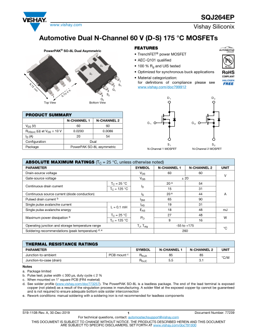
PowerPAK® SO-8L Dual Asymmetric
• TrenchFET® power MOSFET
• AEC-Q101 qualified
D1 • 100 % Rg and UIS tested
• Optimized for synchronous buck applications
D2
• Material categorization:
1 for definitions of compliance please see
2 S1 www.vishay.com/doc?99912
m 3 G1
3 m S
1 5.1 4 2
G D 1 D 2
2
Top View Bottom View
PRODUCT SUMMARY
N-CHANNEL 1 N-CHANNEL 2
G 1 G 2
VDS (V) 60 60
RDS(on) (Ω) at VGS = 10 V 0.0200 0.0086
ID (A) 20 54
Configuration Dual
S S
Package PowerPAK SO-8L asymmetric 1 2
N-Channel 1 MOSFET N-Channel 2 MOSFET
ABSOLUTE MAXIMUM RATINGS (TC = 25 °C, unless otherwise noted)
PARAMETER SYMBOL N-CHANNEL 1 N-CHANNEL 2 UNIT
Drain-source voltage VDS 60 60
V
Gate-source voltage VGS ± 20
TC = 25 °C 20 a 54
Continuous drain current ID
TC = 125 °C 15 31
Continuous source current (diode conduction) I 20 a
S 44 A
Pulsed drain current b IDM 65 90
Single pulse avalanche current IAS 19 31
L = 0.1 mH
Single pulse avalanche energy EAS 18 48 mJ
TC = 25 °C 27 48
Maximum power dissipation b PD W
TC = 125 °C 9 16
Operating junction and storage temperature range TJ, Tstg -55 to +175
°C
Soldering recommendations (peak temperature) d, e 260
THERMAL RESISTANCE RATINGS
PARAMETER SYMBOL N-CHANNEL 1 N-CHANNEL 2 UNIT
Junction-to-ambient PCB mount c RthJA 85 85
°C/W
Junction-to-case (drain) RthJC 5.5 3.1
Notes
a. Package limited
b. Pulse test; pulse width ≤ 300 μs, duty cycle ≤ 2 %
c. When mounted on 1" square PCB (FR4 material)
d. See solder profile (www.vishay.com/doc?73257). The PowerPAK SO-8L is a leadless package. The end of the lead terminal is expose d
copper (not plated) as a result of the singulation process in manufacturing. A solder fillet at the exposed copper tip cannot be guarantee d
and is not required to ensure adequate bottom side solder interconnection
e. Rework conditions: manual soldering with a soldering iron is not recommended for leadless components
S19-1108-Rev. A, 30-Dec-2019 1 Document Number: 77239
For technical questions, contact: automostechsupport@vishay.com
THIS DOCUMENT IS SUBJECT TO CHANGE WITHOUT NOTICE. THE PRODUCTS DESCRIBED HEREIN AND THIS DOCUMENT
ARE SUBJECT TO SPECIFIC DISCLAIMERS, SET FORTH AT www.vishay.com/doc?91000
m
m
6.1
5
Page2
SQJ264EP
www.vishay.com Vishay Siliconix
SPECIFICATIONS (TC = 25 °C, unless otherwise noted)
PARAMETER SYMBOL TEST CONDITIONS MIN. TYP. MAX. UNIT
Static
VGS = 0 V, ID = 250 μA N-Ch 1 60 - -
Drain-source breakdown voltage VDS
VGS = 0 V, ID = 250 μA N-Ch 2 60 - -
V
VDS = VGS, ID = 250 μA N-Ch 1 2.5 3.0 3.5
Gate-source threshold voltage VGS(th)
VDS = VGS, ID = 250 μA N-Ch 2 2.5 3.0 3.5
N-Ch 1 - - ± 100
Gate-source leakage IGSS VDS = 0 V, VGS = ± 20 V nA
N-Ch 2 - - ± 100
VGS = 0 V VDS = 60 V N-Ch 1 - - 1
VGS = 0 V VDS = 60 V N-Ch 2 - - 1
VGS = 0 V VDS = 60 V, TJ = 125 °C N-Ch 1 - - 50
Zero gate voltage drain current IDSS μA
VGS = 0 V VDS = 60 V, TJ = 125 °C N-Ch 2 - - 50
VGS = 0 V VDS = 60 V, TJ = 175 °C N-Ch 1 - - 250
VGS = 0 V VDS = 60 V, TJ = 175 °C N-Ch 2 - - 250
VGS = 10 V VDS ≥ 5 V N-Ch 1 15 - -
On-state drain current a ID(on) A
VGS = 10 V VDS ≥ 5 V N-Ch 2 30 - -
VGS = 10 V ID = 6 A N-Ch 1 - 0.0165 0.0200
VGS = 10 V ID = 10 A N-Ch 2 - 0.0071 0.0086
V = 10 V I = 6 A, T = 125 °C N-Ch 1 - - 0.0320
Drain-source on-state resistance a GS D J
RDS(on) Ω
VGS = 10 V ID = 10 A, TJ = 125 °C N-Ch 2 - - 0.0135
VGS = 10 V ID = 6 A, TJ = 175 °C N-Ch 1 - - 0.0390
VGS = 10 V ID = 10 A, TJ = 175 °C N-Ch 2 - - 0.0167
V = 10 V, I = 6 A N-Ch 1 - 24 -
Forward transconductance b DS D
gfs S
VDS = 10 V, ID = 10 A N-Ch 2 - 98 -
Dynamic b
VGS = 0 V VDS = 25 V, f = 1 MHz N-Ch 1 - 687 1000
Input capacitance Ciss
VGS = 0 V VDS = 25 V, f = 1 MHz N-Ch 2 - 1490 2100
VGS = 0 V VDS = 25 V, f = 1 MHz N-Ch 1 - 313 500
Output capacitance Coss pF
VGS = 0 V VDS = 25 V, f = 1 MHz N-Ch 2 - 777 1100
VGS = 0 V VDS = 25 V, f = 1 MHz N-Ch 1 - 10 15
Reverse transfer capacitance Crss
VGS = 0 V VDS = 25 V, f = 1 MHz N-Ch 2 - 21 30
VGS = 10 V VDS = 30 V, ID = 1.5 A N-Ch 1 - 9.2 16
Total gate charge c Qg
VGS = 10 V VDS = 30 V, ID = 3 A N-Ch 2 - 19.2 32
VGS = 10 V VDS = 30 V, ID = 1.5 A N-Ch 1 - 3.2 - nC
Gate-source charge c Qgs
VGS = 10 V VDS = 30 V, ID = 3 A N-Ch 2 - 6.3 -
VGS = 10 V VDS = 30 V, ID = 1.5 A N-Ch 1 - 0.8 -
Gate-drain charge c Qgd
VGS = 10 V VDS = 30 V, ID = 3 A N-Ch 2 - 1.5 -
N-Ch 1 0.35 0.74 1.20
Gate resistance Rg f = 1 MHz Ω
N-Ch 2 0.20 0.42 0.65
S19-1108-Rev. A, 30-Dec-2019 2 Document Number: 77239
For technical questions, contact: automostechsupport@vishay.com
THIS DOCUMENT IS SUBJECT TO CHANGE WITHOUT NOTICE. THE PRODUCTS DESCRIBED HEREIN AND THIS DOCUMENT
ARE SUBJECT TO SPECIFIC DISCLAIMERS, SET FORTH AT www.vishay.com/doc?91000
Page3
SQJ264EP
www.vishay.com Vishay Siliconix
SPECIFICATIONS (TC = 25 °C, unless otherwise noted)
PARAMETER SYMBOL TEST CONDITIONS MIN. TYP. MAX. UNIT
Dynamic b
VDD = 30 V, RL = 20 Ω,
I ≅ 1.5 A, V = 10 V, R = 1 Ω N-Ch 1 - 11 18
Turn-on delay time c D GEN g
td(on)
VDD = 30 V, RL = 10 Ω,
ID ≅ 3 A, V = 10 V, R = 1 Ω N-Ch 2 - 12 25
GEN g
VDD = 30 V, RL = 20 Ω,
ID ≅ 1.5 A, V = 10 V, R = 1 Ω N-Ch 1 - 2 5
GEN g
Rise time c tr
VDD = 30 V, RL = 10 Ω,
ID ≅ 3 A, VGEN = 10 V, Rg = 1 Ω N-Ch 2 - 3 5
ns
VDD = 30 V, RL = 20 Ω,
ID ≅ 1.5 A, V N-Ch 1 - 16 30
c GEN = 10 V, Rg = 1 Ω
Turn-off delay time td(off)
VDD = 30 V, RL = 10 Ω,
ID ≅ 3 A, VGEN = 10 V, Rg = 1 Ω N-Ch 2 - 20 40
VDD = 30 V, RL = 20 Ω,
ID ≅ 1.5 A, VGEN = 10 V, R = 1 Ω N-Ch 1 - 8 15
g
Fall time c tf
VDD = 30 V, RL = 10 Ω,
ID ≅ 3 A, VGEN = 10 V, R = 1 Ω N-Ch 2 - 11 18
g
Source-Drain Diode Ratings and Characteristics b
N-Ch 1 - - 65
Pulsed current a ISM A
N-Ch 2 - - 90
IF = 6 A, VGS = 0 V N-Ch 1 - 0.82 1.2
Forward voltage VSD V
IF = 10 A, VGS = 0 V N-Ch 2 - 0.80 1.2
IF = 4 A, di/dt = 100 A/μs N-Ch 1 - 22 45
Body diode reverse recovery time trr ns
IF = 5 A, di/dt = 100 A/μs N-Ch 2 - 41 85
IF = 4 A, di/dt = 100 A/μs N-Ch 1 - 15 30
Body diode reverse recovery charge Qrr nC
IF = 5 A, di/dt = 100 A/μs N-Ch 2 - 36 75
IF = 4 A, di/dt = 100 A/μs N-Ch 1 - 12 -
Reverse recovery fall time ta
IF = 5 A, di/dt = 100 A/μs N-Ch 2 - 19 -
ns
IF = 4 A, di/dt = 100 A/μs N-Ch 1 - 10 -
Reverse recovery rise time tb
IF = 5 A, di/dt = 100 A/μs N-Ch 2 - 22 -
Body diode peak reverse recovery IF = 4 A, di/dt = 100 A/μs N-Ch 1 - -1.3 -
current IRM(REC) A
IF = 5 A, di/dt = 100 A/μs N-Ch 2 - -1.6 -
Notes
a. Pulse test; pulse width ≤ 300 μs, duty cycle ≤ 2 %
b. Guaranteed by design, not subject to production testing
c. Independent of operating temperature
Stresses beyond those listed under “Absolute Maximum Ratings” may cause permanent damage to the device. These are stress ratings only, and functional operation
of the device at these or any other conditions beyond those indicated in the operational sections of the specifications is not implied. Exposure to absolute maximum
rating conditions for extended periods may affect device reliability.
S19-1108-Rev. A, 30-Dec-2019 3 Document Number: 77239
For technical questions, contact: automostechsupport@vishay.com
THIS DOCUMENT IS SUBJECT TO CHANGE WITHOUT NOTICE. THE PRODUCTS DESCRIBED HEREIN AND THIS DOCUMENT
ARE SUBJECT TO SPECIFIC DISCLAIMERS, SET FORTH AT www.vishay.com/doc?91000
Page4
SQJ264EP
www.vishay.com Vishay Siliconix
N-CHANNEL 1 TYPICAL CHARACTERISTICS (TA = 25 °C, unless otherwise noted)
Axis Title Axis Title
80 10000 0.10 10000
64 VGS = 10 V thru 7 V 0.08
1000 1000
48 0.06
VGS = 6 V
32 0.04
100 100
VGS = 5 V V
16 GS = 10 V
0.02
VGS = 4 V
0 10 0.00 10
0 2 4 6 8 10 0 10 20 30 40 50
VDS - Drain-to-Source Voltage (V) ID - Drain Current (A)
Output Characteristics Transconductance
Axis Title Axis Title
70 10000 10 000 10000
56
1000 Ciss
1000 C 1000
42 oss
100
28 TC = 25 °C
100 100
10 Crss
14
TC = -55 °C
TC = 125 °C
0 10 1 10
0 2 4 6 8 10 0 12 24 36 48 60
VGS - Gate-to-Source Voltage (V) VDS - Drain-to-Source Voltage (V)
Transfer Characteristics Capacitance
Axis Title Axis Title
50 10000 10 10000
T = -55 °C ID = 1.5 A,
C VDS = 30 V
40 8
TC = 25 °C
1000 1000
30 6
TC = 125 °C
20 4
100 100
10 2
0 10 0 10
0 3 6 9 12 15 0 3 6 9 12 15
ID - Drain Current (A) Qg - Total Gate Charge (nC)
On-Resistance vs. Drain Current Gate Charge
S19-1108-Rev. A, 30-Dec-2019 4 Document Number: 77239
For technical questions, contact: automostechsupport@vishay.com
THIS DOCUMENT IS SUBJECT TO CHANGE WITHOUT NOTICE. THE PRODUCTS DESCRIBED HEREIN AND THIS DOCUMENT
ARE SUBJECT TO SPECIFIC DISCLAIMERS, SET FORTH AT www.vishay.com/doc?91000
2nd line 2nd line 2nd line
gfs - Transconductance (S) ID - Drain Current (A) ID - Drain Current (A)
1st line 1st line 1st line
2nd line 2nd line 2nd line
2nd line 2nd line 2nd line
VGS - Gate-to-Source Voltage (V) C - Capacitance (pF) RDS(on) - On-Resistance (Ω)
1st line 1st line 1st line
2nd line 2nd line 2nd line
Page5
SQJ264EP
www.vishay.com Vishay Siliconix
N-CHANNEL 1 TYPICAL CHARACTERISTICS (TA = 25 °C, unless otherwise noted)
Axis Title Axis Title
2.0 10000 0.10 10000
1.7 ID = 4 A 0.08
1000 1000
1.4 VGS = 10 V 0.06
1.1 0.04
100 TJ = 150 °C 100
0.8 0.02
TJ = 25 °C
0.5 10 0.00 10
-50 -25 0 25 50 75 100 125 150 175 0 2 4 6 8 10
TJ - Junction Temperature (°C) VGS - Gate-to-Source Voltage (V)
Source Drain Diode Forward Voltage On-Resistance vs. Gate-to-Source Voltage
Axis Title Axis Title
76 10000 0.5 10000
ID = 1 mA
74 0.1
1000 1000
72 -0.3
ID = 5 mA
70 -0.7
100 100
68 -1.1 ID = 250 μA
66 10 -1.5 10
-50 -25 0 25 50 75 100 125 150 175 -50 -25 0 25 50 75 100 125 150 175
TJ - Junction Temperature (°C) TJ - Junction Temperature (°C)
Threshold Voltage Drain Source Breakdown vs. Junction Temperature
Axis Title Axis Title
100 10000 100 10000
TJ = 150 °C IDM limited
10 10 100 μs
1000 1000
ID limited 1 ms
1 1 10 ms
TJ = 25 °C 100 ms, 1 s,
Limited by R a
100 DS(on) 10 s1, 0D0C
0.1 0.1 BVDSS limited
TC = 25 °C,
single pulse
0.01 10 0.01 10
0 0.2 0.4 0.6 0.8 1.0 1.2 0.01 0.1 1 10 100
VSD - Source-to-Drain Voltage (V) VDS - Drain-to-Source Voltage (V)
On-Resistance vs. Junction Temperature Safe Operating Area
S19-1108-Rev. A, 30-Dec-2019 5 Document Number: 77239
For technical questions, contact: automostechsupport@vishay.com
THIS DOCUMENT IS SUBJECT TO CHANGE WITHOUT NOTICE. THE PRODUCTS DESCRIBED HEREIN AND THIS DOCUMENT
ARE SUBJECT TO SPECIFIC DISCLAIMERS, SET FORTH AT www.vishay.com/doc?91000
2nd line 2nd line 2nd line
IS - Source Current (A) VDS - Drain-to-Source Voltage (V) RDS(on) - On-Resistance (Normalized)
1st line 1st line 1st line
2nd line 2nd line 2nd line
2nd line 2nd line 2nd line
ID - Drain Current (A) VGS(th) - Variance (V) RDS(on) - On-Resistance (Ω)
1st line 1st line 1st line
2nd line 2nd line 2nd line
Page6
SQJ264EP
www.vishay.com Vishay Siliconix
N-CHANNEL 1 TYPICAL CHARACTERISTICS (TA = 25 °C, unless otherwise noted)
Axis Title
10000
1
Duty cycle = 0.5
0.2 1000
Notes
0.1 PDM
0.1
0.05 t1
t 100
2
t
0.02 1. Duty cycle, D = 1
t2
2. Per unit base = RthJA = 85 °C/W
Single pulse 3. TJM - TA = P (t)
DMZthJA
4. Surface mounted
0.01 10
0.0001 0.001 0.01 0.1 1 10 100 1000
Square Wave Pulse Duration (s)
Normalized Thermal Transient Impedance, Junction-to-Ambient
Axis Title
10000
1
Duty cycle = 0.5
0.2 1000
0.1
0.1
0.05 100
Single pulse 0.02
0.01 10
0.0001 0.001 0.01 0.1 1 10
Square Wave Pulse Duration (s)
Normalized Thermal Transient Impedance, Junction-to-Case
Note
• The characteristics shown in the graph:
- Normalized Transient Thermal Impedance Junction-to-Ambient (25 °C)
is given for general guidelines only to enable the user to get a “ball park” indication of part capabilities. The data are extracted from singl e
pulse transient thermal impedance characteristics which are developed from empirical measurements. The latter is valid for the par t
mounted on printed circuit board - FR4, size 1" x 1" x 0.062", double sided with 2 oz. copper, 100 % on both sides. The part capabilities
can widely vary depending on actual application parameters and operating conditions
S19-1108-Rev. A, 30-Dec-2019 6 Document Number: 77239
For technical questions, contact: automostechsupport@vishay.com
THIS DOCUMENT IS SUBJECT TO CHANGE WITHOUT NOTICE. THE PRODUCTS DESCRIBED HEREIN AND THIS DOCUMENT
ARE SUBJECT TO SPECIFIC DISCLAIMERS, SET FORTH AT www.vishay.com/doc?91000
Normalized Effective Transient Normalized Effective Transient
Thermal Impedance Thermal Impedance
1st line 1st line
2nd line 2nd line
Page7
SQJ264EP
www.vishay.com Vishay Siliconix
N-CHANNEL 2 TYPICAL CHARACTERISTICS (TA = 25 °C, unless otherwise noted)
Axis Title Axis Title
100 10000 0.025 10000
VGS = 10 V thru 6 V
80 VGS = 5 V 0.020
1000 1000
60 0.015
40 0.010 VGS = 10 V
100 100
VGS = 4 V
20 0.005
0 10 0 10
0 2 4 6 8 10 0 16 32 48 64 80
VDS - Drain-to-Source Voltage (V) ID - Drain Current (A)
Output Characteristics Transconductance
Axis Title Axis Title
80 10000 10 000 10000
64 Ciss
1000 1000 Coss 1000
48
TC = 25 °C
32
100 100 100
16
TC = 125 °C Crss
TC = -55 °C
0 10 10 10
0 2 4 6 8 10 0 12 24 36 48 60
VGS - Gate-to-Source Voltage (V) VDS - Drain-to-Source Voltage (V)
Transfer Characteristics Capacitance
Axis Title Axis Title
150 10000 10 10000
TC = -55 °C
120 8 ID = 3 A,
TC = 25 °C VDS = 30 V
1000 1000
90 6
TC = 125 °C
60 4
100 100
30 2
0 10 0 10
0 3 6 9 12 15 0 6 12 18 24 30
ID - Drain Current (A) Qg - Total Gate Charge (nC)
On-Resistance vs. Drain Current Gate Charge
S19-1108-Rev. A, 30-Dec-2019 7 Document Number: 77239
For technical questions, contact: automostechsupport@vishay.com
THIS DOCUMENT IS SUBJECT TO CHANGE WITHOUT NOTICE. THE PRODUCTS DESCRIBED HEREIN AND THIS DOCUMENT
ARE SUBJECT TO SPECIFIC DISCLAIMERS, SET FORTH AT www.vishay.com/doc?91000
2nd line 2nd line 2nd line
gfs - Transconductance (S) ID - Drain Current (A) ID - Drain Current (A)
1st line 1st line 1st line
2nd line 2nd line 2nd line
2nd line 2nd line 2nd line
VGS - Gate-to-Source Voltage (V) C - Capacitance (pF) RDS(on) - On-Resistance (Ω)
1st line 1st line 1st line
2nd line 2nd line 2nd line
Page8
SQJ264EP
www.vishay.com Vishay Siliconix
N-CHANNEL 2 TYPICAL CHARACTERISTICS (TA = 25 °C, unless otherwise noted)
Axis Title Axis Title
2.0 10000 0.05 10000
1.7 ID = 8 A 0.04
1000 1000
1.4 VGS = 10 V 0.03
1.1 0.02
100 TJ = 150 °C 100
0.8 0.01
TJ = 25 °C
0.5 10 0.00 10
-50 -25 0 25 50 75 100 125 150 175 0 2 4 6 8 10
TJ - Junction Temperature (°C) VGS - Gate-to-Source Voltage (V)
Source Drain Diode Forward Voltage On-Resistance vs. Gate-to-Source Voltage
Axis Title Axis Title
73 10000 0.5 10000
ID = 1 mA
71 0.1
1000 1000
69 -0.3
ID = 5 mA
67 -0.7
100 100
ID = 250 μA
65 -1.1
63 10 -1.5 10
-50 -25 0 25 50 75 100 125 150 175 -50 -25 0 25 50 75 100 125 150 175
TJ - Junction Temperature (°C) TJ - Junction Temperature (°C)
Threshold Voltage Drain Source Breakdown vs. Junction Temperature
Axis Title Axis Title
100 10000 1000 10000
IDM limited
T 100
10 J = 150 °C
1000 100 1μ0s00
10
1 1 ms
TJ = 25 °C 1 10 ms
100 Limited by R a
DS(on) 100 ms, 1 s,
10 s1, 0D0C
0.1 BVDSS limited
0.1
TC = 25 °C,
single pulse
0.01 10 0.01 10
0 0.2 0.4 0.6 0.8 1.0 1.2 0.01 0.1 1 10 100
VSD - Source-to-Drain Voltage (V) VDS - Drain-to-Source Voltage (V)
On-Resistance vs. Junction Temperature Safe Operating Area
S19-1108-Rev. A, 30-Dec-2019 8 Document Number: 77239
For technical questions, contact: automostechsupport@vishay.com
THIS DOCUMENT IS SUBJECT TO CHANGE WITHOUT NOTICE. THE PRODUCTS DESCRIBED HEREIN AND THIS DOCUMENT
ARE SUBJECT TO SPECIFIC DISCLAIMERS, SET FORTH AT www.vishay.com/doc?91000
2nd line 2nd line 2nd line
IS - Source Current (A) VDS - Drain-to-Source Voltage (V) RDS(on) - On-Resistance (Normalized)
1st line 1st line 1st line
2nd line 2nd line 2nd line
2nd line 2nd line 2nd line
ID - Drain Current (A) VGS(th) - Variance (V) RDS(on) - On-Resistance (Ω)
1st line 1st line 1st line
2nd line 2nd line 2nd line
Page9
SQJ264EP
www.vishay.com Vishay Siliconix
N-CHANNEL 2 TYPICAL CHARACTERISTICS (TA = 25 °C, unless otherwise noted)
Axis Title
10000
1
Duty cycle = 0.5
0.2 1000
Notes
0.1 PDM
0.1
0.05 t1
t 100
2
t
0.02 1. Duty cycle, D = 1
t2
2. Per unit base = RthJA = 85 °C/W
(t)
Single pulse 3. TJM - TA = PDMZthJA
4. Surface mounted
0.01 10
0.0001 0.001 0.01 0.1 1 10 100 1000
Square Wave Pulse Duration (s)
Normalized Thermal Transient Impedance, Junction-to-Ambient
Axis Title
10000
1
Duty cycle = 0.5
0.2 1000
0.1 0.1
0.05 100
0.02
Single pulse
0.01 10
0.0001 0.001 0.01 0.1 1 10
Square Wave Pulse Duration (s)
Normalized Thermal Transient Impedance, Junction-to-Case
Note
• The characteristics shown in the graph:
- Normalized Transient Thermal Impedance Junction-to-Ambient (25 °C)
is given for general guidelines only to enable the user to get a “ball park” indication of part capabilities. The data are extracted from singl e
pulse transient thermal impedance characteristics which are developed from empirical measurements. The latter is valid for the par t
mounted on printed circuit board - FR4, size 1" x 1" x 0.062", double sided with 2 oz. copper, 100 % on both sides. The part capabilities
can widely vary depending on actual application parameters and operating conditions
Vishay Siliconix maintains worldwide manufacturing capability. Products may be manufactured at one of several qualified locations. Reliability data for Silico n
Technology and Package Reliability represent a composite of all qualified locations. For related documents such as package / tape drawings, part marking, and
reliability data, see www.vishay.com/ppg?75486.
S19-1108-Rev. A, 30-Dec-2019 9 Document Number: 77239
For technical questions, contact: automostechsupport@vishay.com
THIS DOCUMENT IS SUBJECT TO CHANGE WITHOUT NOTICE. THE PRODUCTS DESCRIBED HEREIN AND THIS DOCUMENT
ARE SUBJECT TO SPECIFIC DISCLAIMERS, SET FORTH AT www.vishay.com/doc?91000
Normalized Effective Transient Normalized Effective Transient
Thermal Impedance Thermal Impedance
1st line 1st line
2nd line 2nd line
Page10
Package Information
www.vishay.com Vishay Siliconix
PowerPAK® SO-8L Assymetric Case Outline
b2 D5
D4 K1 D3
D2
A1
b b1 e θ
D1 b3 K2
D 0.25 gauge line PIN 1
PIN 1
MILLIMETERS INCHES
DIM.
MIN. NOM. MAX. MIN. NOM. MAX.
A 1.00 1.07 1.14 0.039 0.042 0.045
A1 0.00 0.06 0.13 0.000 0.003 0.005
b 0.33 0.41 0.48 0.013 0.016 0.019
b1 0.44 0.51 0.58 0.017 0.020 0.023
b2 4.80 4.90 5.00 0.189 0.193 0.197
b3 0.04 0.12 0.20 0.002 0.005 0.008
c 0.20 0.25 0.30 0.008 0.010 0.012
D 5.00 5.13 5.25 0.197 0.202 0.207
D1 4.80 4.90 5.00 0.189 0.193 0.197
D2 3.63 3.73 3.83 0.143 0.147 0.151
D3 0.81 0.91 1.01 0.032 0.036 0.040
D4 1.98 2.08 2.18 0.078 0.082 0.086
D5 1.47 1.57 1.67 0.058 0.062 0.066
e 1.20 1.27 1.34 0.047 0.050 0.053
E 6.05 6.15 6.25 0.238 0.242 0.246
E1 4.27 4.37 4.47 0.168 0.172 0.176
E2 2.75 2.85 2.95 0.108 0.112 0.116
E3 1.89 1.99 2.09 0.074 0.078 0.082
F 0.05 0.12 0.19 0.002 0.005 0.007
L 0.62 0.72 0.82 0.024 0.028 0.032
L1 0.92 1.07 1.22 0.036 0.042 0.048
K 0.41 0.51 0.61 0.016 0.020 0.024
K1 0.64 0.74 0.84 0.025 0.029 0.033
K2 0.54 0.64 0.74 0.021 0.025 0.029
W 0.13 0.23 0.33 0.005 0.009 0.013
W1 0.31 0.41 0.51 0.012 0.016 0.020
W2 2.72 2.82 2.92 0.107 0.111 0.115
W3 2.86 2.96 3.06 0.113 0.117 0.120
W4 0.41 0.51 0.61 0.016 0.020 0.024
θ 5° 10° 12° 5° 10° 12°
DWG: 6009
Note
• Millimeters will govern
C14-0057-Rev. D, 07-Apr-14 1 Document Number: 62714
For technical questions, contact: pmostechsupport@vishay.com
THIS DOCUMENT IS SUBJECT TO CHANGE WITHOUT NOTICE. THE PRODUCTS DESCRIBED HEREIN AND THIS DOCUMENT
ARE SUBJECT TO SPECIFIC DISCLAIMERS, SET FORTH AT www.vishay.com/doc?91000
Page11
PAD Pattern
www.vishay.com Vishay Siliconix
RECOMMENDED MINIMUM PADs FOR PowerPAK® SO-8L DUAL ASYMMETRIC
Recommended Minimum Pads
Dimensions in mm [inches]
Revision: 07-Mar-13 1 Document Number: 64477
THIS DOCUMENT IS SUBJECT TO CHANGE WITHOUT NOTICE. THE PRODUCTS DESCRIBED HEREIN AND THIS DOCUMENT
ARE SUBJECT TO SPECIFIC DISCLAIMERS, SET FORTH AT www.vishay.com/doc?91000
Page12
Legal Disclaimer Notice
www.vishay.com Vishay
Disclaimer
ALL PRODUCT, PRODUCT SPECIFICATIONS AND DATA ARE SUBJECT TO CHANGE WITHOUT NOTICE TO IMPROV E
RELIABILITY, FUNCTION OR DESIGN OR OTHERWISE.
Vishay Intertechnology, Inc., its affiliates, agents, and employees, and all persons acting on its or their behalf (collectively ,
“Vishay”), disclaim any and all liability for any errors, inaccuracies or incompleteness contained in any datasheet or in any other
disclosure relating to any product.
Vishay makes no warranty, representation or guarantee regarding the suitability of the products for any particular purpose o r
the continuing production of any product. To the maximum extent permitted by applicable law, Vishay disclaims (i) any and all
liability arising out of the application or use of any product, (ii) any and all liability, including without limitation special,
consequential or incidental damages, and (iii) any and all implied warranties, including warranties of fitness for particular
purpose, non-infringement and merchantability.
Statements regarding the suitability of products for certain types of applications are based on Vishay's knowledge of typical
requirements that are often placed on Vishay products in generic applications. Such statements are not binding statement s
about the suitability of products for a particular application. It is the customer's responsibility to validate that a particular produc t
with the properties described in the product specification is suitable for use in a particular application. Parameters provided in
datasheets and / or specifications may vary in different applications and performance may vary over time. All operatin g
parameters, including typical parameters, must be validated for each customer application by the customer's technical experts.
Product specifications do not expand or otherwise modify Vishay's terms and conditions of purchase, including but not limited
to the warranty expressed therein.
Hyperlinks included in this datasheet may direct users to third-party websites. These links are provided as a convenience and
for informational purposes only. Inclusion of these hyperlinks does not constitute an endorsement or an approval by Vishay of
any of the products, services or opinions of the corporation, organization or individual associated with the third-party website .
Vishay disclaims any and all liability and bears no responsibility for the accuracy, legality or content of the third-party website
or for that of subsequent links.
Except as expressly indicated in writing, Vishay products are not designed for use in medical, life-saving, or life-sustainin g
applications or for any other application in which the failure of the Vishay product could result in personal injury or death.
Customers using or selling Vishay products not expressly indicated for use in such applications do so at their own risk. Please
contact authorized Vishay personnel to obtain written terms and conditions regarding products designed for such applications.
No license, express or implied, by estoppel or otherwise, to any intellectual property rights is granted by this document or by
any conduct of Vishay. Product names and markings noted herein may be trademarks of their respective owners.
© 2022 VISHAY INTERTECHNOLOGY, INC. ALL RIGHTS RESERVED
Revision: 01-Jan-2022 1 Document Number: 91000