


Fully Integrated Proximity and Ambient Light Sensor With Infrared Emitter, I2C Interface, and Interrupt Function(with multiple slave addresses)
このカタログについて
| ドキュメント名 | Vishay Semiconductors VCNL4030X01 |
|---|---|
| ドキュメント種別 | 製品カタログ |
| ファイルサイズ | 309.8Kb |
| 取り扱い企業 | マウザー・エレクトロニクス (この企業の取り扱いカタログ一覧) |
この企業の関連カタログ


このカタログの内容
Page1
VCNL4030X01
www.vishay.com Vishay Semiconductors
Fully Integrated Proximity and Ambient Light Sensor With
Infrared Emitter, I2C Interface, and Interrupt Function
(with multiple slave addresses)
FEATURES
• Package type: surface-mount
• Dimensions (L x W x H in mm): 4.0 x 2.36 x 0.75
• AEC-Q101 qualified
• Integrated modules: infrared emitter (IRED),
ambient light sensor (ALS), proximity sensor
(PS), and signal conditioning IC
• Operates ALS and PS in parallel structure
• FiltronTM technology adoption for robus t
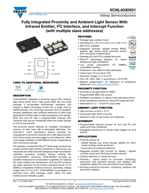
VDD 1 8 SDA background light cancellation
• Low power consumption I2C (SMBus
SCL 2 7 INT
compatible) interface
GND 3 6 LDR • Orderable in four different slave addresses
IR anode 4 5 IR cathode • Output type: I2C bus (ALS / PS)
• Operation voltage: 2.5 V to 3.6 V
• Floor life: 168 h, MSL 3, according to J-STD-020
LINKS TO ADDITIONAL RESOURCES • Material categorization: for definitions of complianc e
please see www.vishay.com/doc?99912
3D 3D PROXIMITY FUNCTION
3D Models Design Tools Related
Documents • Immunity to red glow (940 nm IRED)
DESCRIPTION • Programmable IRED sink current
• Intelligent cancellation to reduce cross talk phenomenon
VCNL4030X01 integrates a proximity sensor (PS), ambient
light sensor (ALS), and a high power IRED into one small • Smart persistence scheme to reduce PS response time
package. It incorporates photodiodes, amplifiers, an d • Selectable for 12- / 16-bit PS output data
analog to digital converting circuits into a single chip b y AMBIENT LIGHT FUNCTION
CMOS process. The 16-bit high resolution ALS for excellent • High accuracy of ALS ± 10 %
sensing capabilities with sufficient selections to fulfill most
applications whether dark or high transparency lens design . • Fluorescent light flicker immunity
Both ALS and PS offer a programmable interrupt with • Spectrum close to real human eye responses
individual high and low thresholds offers the power savings INTERRUPT
on the microcontroller. • Programmable interrupt function for ALS and PS with
The proximity sensor features an intelligent cancellation upper and lower thresholds
scheme, so that cross talk is eliminated effectively. The • Adjustable persistence to prevent false triggers for ALS
proximity’s smart persistence feature prevents th e and PS
misjudgment of proximity sensing with a fast response time.
Active force mode, one time trigger by one instruction, offer s APPLICATIONS
more design flexibility to fulfill different kinds of applications • Proximity sensor for
with more power savings. - Mobile devices (e.g. smart phones, tablets) for touch
The adoption of patented FiltronTM technology achieves the screen locking, power saving etc.
closest ambient light spectral sensitivity to real human ey e - Automotive for presence detection
responses and offers the best background light cancellatio n • Integrated ambient light function for display / keypad
capability (including sunlight) without utilizing the contrast control and dimming of mobile devices
microcontrollers’ resources. VCNL4030X01 provides an • Collision detection in robots and toys
excellent temperature compensation capability for keeping • Proximity / optical switch for consumer, computing,
the output stable over temperature. ALS and PS functions automotive and industrial devices, and displays (lik e
are easily operated via the simple command format of I2C notebooks, tablet PCs, and automotive touch panels)
(SMBus compatible) interface protocol. Operating voltag e • Dimming control for consumer, computing, industrial, an d
ranges from 2.5 V to 3.6 V. VCNL4030X01 is packaged in a automotive displays
lead-free 8-pin QFN package, which offers the best
market-proven reliability quality.
Rev. 1.2, 18-Mar-2020 1 Document Number: 84250
For technical questions, contact: sensorstechsupport@vishay.com
THIS DOCUMENT IS SUBJECT TO CHANGE WITHOUT NOTICE. THE PRODUCTS DESCRIBED HEREIN AND THIS DOCUMENT
ARE SUBJECT TO SPECIFIC DISCLAIMERS, SET FORTH AT www.vishay.com/doc?91000
Page2
VCNL4030X01
www.vishay.com Vishay Semiconductors
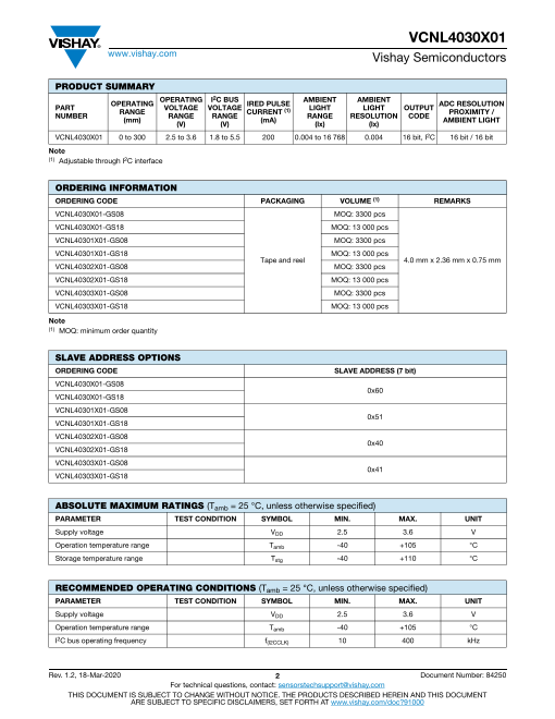
PRODUCT SUMMARY
OPERATING I2C BUS AMBIENT AMBIENT
PART OPERATING VOLTAGE VOLTAGE IRED PULSE ADC RESOLUTION
NUMBER RANGE RANGE RANGE CURRENT (1) LIGHT LIGHT OUTPUT
(mm) (mA) RANGE RESOLUTION CODE PROXIMITY /
(V) (V) (lx) (lx) AMBIENT LIGHT
VCNL4030X01 0 to 300 2.5 to 3.6 1.8 to 5.5 200 0.004 to 16 768 0.004 16 bit, I2C 16 bit / 16 bit
Note
(1) Adjustable through I2C interface
ORDERING INFORMATION
ORDERING CODE PACKAGING VOLUME (1) REMARKS
VCNL4030X01-GS08 MOQ: 3300 pcs
VCNL4030X01-GS18 MOQ: 13 000 pcs
VCNL40301X01-GS08 MOQ: 3300 pcs
VCNL40301X01-GS18 MOQ: 13 000 pcs
Tape and reel 4.0 mm x 2.36 mm x 0.75 mm
VCNL40302X01-GS08 MOQ: 3300 pcs
VCNL40302X01-GS18 MOQ: 13 000 pcs
VCNL40303X01-GS08 MOQ: 3300 pcs
VCNL40303X01-GS18 MOQ: 13 000 pcs
Note
(1) MOQ: minimum order quantity
SLAVE ADDRESS OPTIONS
ORDERING CODE SLAVE ADDRESS (7 bit)
VCNL4030X01-GS08
0x60
VCNL4030X01-GS18
VCNL40301X01-GS08
0x51
VCNL40301X01-GS18
VCNL40302X01-GS08
0x40
VCNL40302X01-GS18
VCNL40303X01-GS08
0x41
VCNL40303X01-GS18
ABSOLUTE MAXIMUM RATINGS (Tamb = 25 °C, unless otherwise specified)
PARAMETER TEST CONDITION SYMBOL MIN. MAX. UNIT
Supply voltage VDD 2.5 3.6 V
Operation temperature range Tamb -40 +105 °C
Storage temperature range Tstg -40 +110 °C
RECOMMENDED OPERATING CONDITIONS (Tamb = 25 °C, unless otherwise specified)
PARAMETER TEST CONDITION SYMBOL MIN. MAX. UNIT
Supply voltage VDD 2.5 3.6 V
Operation temperature range Tamb -40 +105 °C
I2C bus operating frequency f(I2CCLK) 10 400 kHz
Rev. 1.2, 18-Mar-2020 2 Document Number: 84250
For technical questions, contact: sensorstechsupport@vishay.com
THIS DOCUMENT IS SUBJECT TO CHANGE WITHOUT NOTICE. THE PRODUCTS DESCRIBED HEREIN AND THIS DOCUMENT
ARE SUBJECT TO SPECIFIC DISCLAIMERS, SET FORTH AT www.vishay.com/doc?91000
Page3
VCNL4030X01
www.vishay.com Vishay Semiconductors
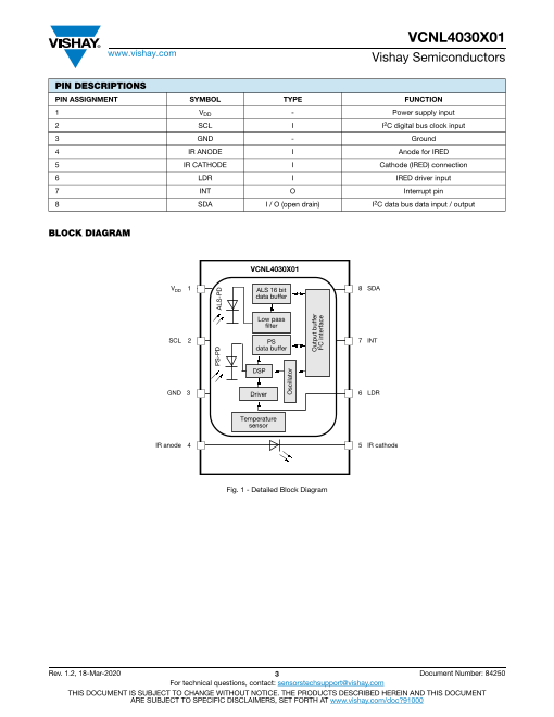
PIN DESCRIPTIONS
PIN ASSIGNMENT SYMBOL TYPE FUNCTION
1 VDD - Power supply input
2 SCL I I2C digital bus clock input
3 GND - Ground
4 IR ANODE I Anode for IRED
5 IR CATHODE I Cathode (IRED) connection
6 LDR I IRED driver input
7 INT O Interrupt pin
8 SDA I / O (open drain) I2C data bus data input / output
BLOCK DIAGRAM
VCNL4030X01
VDD 1 ALS 16 bit 8 SDA
data buffer
Low pass
filter
SCL 2 PS 7 INT
data buffer
DSP
GND 3 Driver 6 LDR
Temperature
sensor
IR anode 4 5 IR cathode
Fig. 1 - Detailed Block Diagram
Rev. 1.2, 18-Mar-2020 3 Document Number: 84250
For technical questions, contact: sensorstechsupport@vishay.com
THIS DOCUMENT IS SUBJECT TO CHANGE WITHOUT NOTICE. THE PRODUCTS DESCRIBED HEREIN AND THIS DOCUMENT
ARE SUBJECT TO SPECIFIC DISCLAIMERS, SET FORTH AT www.vishay.com/doc?91000
PS-PD ALS-PD
Oscillator
Output buffer
I2C interface
Page4
VCNL4030X01
www.vishay.com Vishay Semiconductors
BASIC CHARACTERISTICS (Tamb = 25 °C, unless otherwise specified)
PARAMETER TEST CONDITION SYMBOL MIN. TYP. MAX. UNIT
Supply voltage VDD 2.5 - 3.6 V
Excluded LED driving IDD - 300 - μA
Supply current
Light condition = dark, VDD = 3.3 V IDD (SD) - 0.2 - μA
I2C supply voltage VPULL UP 1.8 - 5.5 V
ALS shut down ALS disable, PS enable IALSSD - 200 - μA
PS shut down ALS enable, PS disable IPSSD - 260 - μA
Logic high VIH 1.55 - -
VDD = 3.3 V V
Logic low V - - 0.4
I2
IL
C signal input
Logic high VIH 1.4 - -
VDD = 2.6 V V
Logic low VIL - - 0.4
Peak sensitivity wavelength of
ALS λp - 550 - nm
Peak sensitivity wavelength of PS λp - 850 - nm
Full ALS counts 16-bit resolution - - 65 535 steps
Full PS counts 12-bit / 16-bit resolution - - 4096 / 65 535 steps
ALS sensing tolerance White LED light source - - ± 10 %
Detectable Minimum ALS_IT = 800 ms, 1 step (1)(2) - 0.004 -
intensity lx
Maximum ALS_IT = 50 ms, 65 535 step (1)(2) - 16 768 -
ALS dark offset ALS_IT = 50 ms, normal sensitivity (1) 0 - 3 steps
PS detection range Kodak gray card 0 - 300 mm
Operating temperature range Tamb -40 - +105 °C
LED_Anode voltage - - 5.5 V
IRED driving current (3) - 200 - mA
Notes
(1) Test condition: VDD = 3.3 V, temperature: 25 °C
(2) Maximum detection range to ambient light can be determined by ALS refresh time adjustment and two sensitivity bits (ALS_HD an d
ALS_NS). Refer to table “ALS Resolution and Maximum Detection Range”
(3) Programmable between 50 mA and 200 mA; based on IRED on / off duty ratio = 1/40, 1/80, 1/160, and 1/320
Rev. 1.2, 18-Mar-2020 4 Document Number: 84250
For technical questions, contact: sensorstechsupport@vishay.com
THIS DOCUMENT IS SUBJECT TO CHANGE WITHOUT NOTICE. THE PRODUCTS DESCRIBED HEREIN AND THIS DOCUMENT
ARE SUBJECT TO SPECIFIC DISCLAIMERS, SET FORTH AT www.vishay.com/doc?91000
Page5
VCNL4030X01
www.vishay.com Vishay Semiconductors
I2C BUS TIMING CHARACTERISTICS (Tamb = 25 °C, unless otherwise specified)
STANDARD MODE FAST MODE
PARAMETER SYMBOL UNIT
MIN. MAX. MIN. MAX.
Clock frequency f(I2CCLK) 10 100 10 400 kHz
Bus free time between start and stop condition t(BUF) 4.7 - 1.3 - μs
Hold time after (repeated) start condition;
after this period, the first clock is generated t(HDSTA) 4.0 - 0.6 - μs
Repeated start condition setup time t(SUSTA) 4.7 - 0.6 - μs
Stop condition setup time t(SUSTO) 4.0 - 0.6 - μs
Data hold time t(HDDAT) - 3450 - 900 ns
Data setup time t(SUDAT) 250 - 100 - ns
I2C clock (SCK) low period t(LOW) 4.7 - 1.3 - μs
I2C clock (SCK) high period t(HIGH) 4.0 - 0.6 - μs
Clock / data fall time tf - 300 - 300 ns
Clock / data rise time tr - 1000 - 300 ns
t(LOW) tr tf
I2C bus VIH
CLOCK
(SCLK) VIL
t(HDSTA) t(HIGH) t(SUSTA)
t(SUSTO)
t(BUF)
t(HDDAT) t(SUDAT)
I2C bus VIH
DATA
(SDAT) VIL
{ { { {
P S S P
Stop condition Start condition
Start Stop
t(LOSEXT)
SCLKACK SDAACK
t(LOWMEXT) t(LOWMEXT) t(LOWMEXT)
I2C bus
CLOCK
(SCLK)
I2C bus
DATA
(SDAT)
Fig. 2 - I2C Bus Timing Diagram
Rev. 1.2, 18-Mar-2020 5 Document Number: 84250
For technical questions, contact: sensorstechsupport@vishay.com
THIS DOCUMENT IS SUBJECT TO CHANGE WITHOUT NOTICE. THE PRODUCTS DESCRIBED HEREIN AND THIS DOCUMENT
ARE SUBJECT TO SPECIFIC DISCLAIMERS, SET FORTH AT www.vishay.com/doc?91000
Page6
VCNL4030X01
www.vishay.com Vishay Semiconductors
PARAMETER TIMING INFORMATION
I2C bus
CLOCK
(SCLK)
I2C bus
DATA SA7 SA6 SA5 SA4 SA3 SA2 SA1
(SDAT) W SA7 SA6 SA5 SA4 SA3 SA2 SA1 SA0
Start by ACK by ACK by
master VCNL4030X01 VCNL4030X01
I2C bus slave address byte Command code
I2C bus
CLOCK
(SCLK)
I2C bus
DATA SA7 SA6 SA5 SA4 SA3 SA2 SA1 SA0 SA7 SA6 SA5 SA4 SA3 SA2 SA1 SA0
(SDAT)
ACK by ACK by Stop by
VCNL4030X01 VCNL4030X01 master
Data byte low Data byte high
Fig. 3 - I2C Bus Timing for Sending Word Command Format
I2C bus
CLOCK
(SCLK)
I2C bus
DATA
(SDAT) SA7 SA6 SA5 SA4 SA3 SA2 SA1 W SA7 SA6 SA5 SA4 SA3 SA2 SA1 SA0
Start by ACK by ACK by
master VCNL4030X01 VCNL4030X01
I2C bus slave address byte Command code
I2C bus
CLOCK
(SCLK)
I2C bus
DATA
SA7 SA6 SA5 SA4 SA3 SA2 SA1 R SA7 SA6 SA5 SA4 SA3 SA2 SA1 SA0
(SDAT)
Start by ACK by ACK by
master VCNL4030X01 master
I2C bus slave address byte Data byte low
I2C bus
CLOCK
(SCLK)
I2C bus
DATA SA7 SA6 SA5 SA4 SA3 SA2 SA1 SA0
(SDAT)
NACK by Stop by
master master
Data byte high
Fig. 4 - I2C Bus Timing for Receiving Word Command Format
Rev. 1.2, 18-Mar-2020 6 Document Number: 84250
For technical questions, contact: sensorstechsupport@vishay.com
THIS DOCUMENT IS SUBJECT TO CHANGE WITHOUT NOTICE. THE PRODUCTS DESCRIBED HEREIN AND THIS DOCUMENT
ARE SUBJECT TO SPECIFIC DISCLAIMERS, SET FORTH AT www.vishay.com/doc?91000
Page7
VCNL4030X01
www.vishay.com Vishay Semiconductors
TYPICAL PERFORMANCE CHARACTERISTICS (Tamb = 25 °C, unless otherwise specified)
Axis Title Axis Title
1.0 10000 0.22 10000
ALS
0.9
V(λ) human eye 0.20 VDD = 3.6 V
rel
0.8
0.7
1000 0.18 VDD = 3.0 V 1000
0.6
0.5 0.16
V
0.4 DD = 2.5 V
100 0.14 100
0.3
0.2 0.12 PS: active force mode enable
0.1 ALS: disabled
0 10 0.10 10
400 500 600 700 800 900 -40 -20 0 20 40 60 80 100 120
λ - Wavelength (nm) Tamb - Ambient Temperature (°C)
2nd line 2nd line
Fig. 5 - Normalized Spectral Response Fig. 8 - Supply Current vs. Ambient Temperature
(ALS channel) With Only PS = Active
Axis Title Axis Title
1.0 10000 0.50 10000
0.9
0.45
0.8
0.7 0.40
1000 V 1000
DD = 3.6 V
0.6 0.35 VDD = 3.0 V
0.5
0.4 0.30
100 VDD = 2.5 V 100
0.3 0.25
0.2
0.20 PS: disabled
0.1 ALS: cont. active, white channel shut down
0 10 0.15 10
500 600 700 800 900 1000 1100 -40 -20 0 20 40 60 80 100 120
λ - Wavelength (nm) Tamb - Ambient Temperature (°C)
2nd line 2nd line
Fig. 6 - Normalized Spectral Response Fig. 9 - Supply Current vs. Ambient Temperature
(PS channel) With Only ALS = Active
Axis Title
0° 20°
10000
t
100 p = 500 μs
Tamb = 25 °C
1.0
1000 0.9 40°
0.8
10
100 0.7
60°
0.6
1 10 80°
0.8 0.9 1.0 1.1 1.2 1.3 1.4 1.5 1.6 1.7
VF - Forward Voltage (V) 0.5 0.4 0.3 0.2 0.1 0
2nd line
Fig. 7 - Forward Current I = f (V ) Fig. 10 - Relative Radiant Intensity Emitter vs.
F F
for LED Angular Displacement
Rev. 1.2, 18-Mar-2020 7 Document Number: 84250
For technical questions, contact: sensorstechsupport@vishay.com
THIS DOCUMENT IS SUBJECT TO CHANGE WITHOUT NOTICE. THE PRODUCTS DESCRIBED HEREIN AND THIS DOCUMENT
ARE SUBJECT TO SPECIFIC DISCLAIMERS, SET FORTH AT www.vishay.com/doc?91000
2nd line 2nd line 2nd line
IF - Forward Current (mA) S(λ)rel - Relative Spectral Sensitivity S(λ)rel - Relative Spectral Sensitivity
1st line 1st line 1st line
2nd line 2nd line 2nd line
2nd line 2nd line
IDD - Supply Current (mA) IDD - Supply Current (mA)Irel - Relative Radiant Intensity
ϕ - Angular Displacement 1st line 1st line
2nd line 2nd line
Page8
VCNL4030X01
www.vishay.com Vishay Semiconductors
Axis Title Axis Title
1.0 10000 1.0 10000
0.9 0.9
0.8 0.8
0.7
1000 0.7
1000
0.6 0.6
0.5 0.5
0.4 0.4
100
0.3 100
0.3
0.2 0.2
0.1 0.1
0 10 0 10
-90 -60 -30 0 30 60 90 400 500 600 700 800 900 1000
ϕ - Angular Displacement (°) Wavelength (nm)
2nd line 2nd line
Fig. 11 - Relative Radiant Intensity Emitter vs. Fig. 14 - White Channel Spectral Response
Angular Displacement
Axis Title
0° 20°
100 000 10000
1.0 10 000
0.9 40° 1000
1000
0.8
0.7 100
100
60°
10
0.6 Media: Kodak Gray Card
(8T and 200 mA)
80° 1 10
0.1 1 10 100 1000
0.5 0.4 0.3 0.2 0.1 0 Distance to Reflection Card (mm)
2nd line
Fig. 12 - Relative Sensitivity vs. Angular Displacement Fig. 15 - Proximity Value vs. Distance to Reflecting Card
(ALS)
Axis Title
1.0 10000
0.9
0.8
0.7
1000
0.6
0.5
0.4
100
0.3
0.2
0.1
0 10
-90 -60 -30 0 30 60 90
ϕ - Angular Displacement (°)
2nd line
Fig. 13 - Relative Sensitivity vs. Angular Displacement
Rev. 1.2, 18-Mar-2020 8 Document Number: 84250
For technical questions, contact: sensorstechsupport@vishay.com
THIS DOCUMENT IS SUBJECT TO CHANGE WITHOUT NOTICE. THE PRODUCTS DESCRIBED HEREIN AND THIS DOCUMENT
ARE SUBJECT TO SPECIFIC DISCLAIMERS, SET FORTH AT www.vishay.com/doc?91000
2nd line 2nd line
Srel - Relative Sensitivity Ie, rel - Relative Radiant IntensitySrel - Relative Sensitivity
1st line ϕ - Angular Displacement 1st line
2nd line 2nd line
2nd line Normalized Output
Proximity Value (cts) 1st line
1st line 1st line
2nd line 2nd line
Page9
VCNL4030X01
www.vishay.com Vishay Semiconductors
APPLICATION INFORMATION
Pin Connection with the Host
VCNL4030X01 integrates proximity sensor, ambient light Sensor, and IRED all together with I2C interface. It is very easy for the
baseband (CPU) to access PS and ALS output data via I2C interface without extra software algorithms. The hardware schematic
is shown in the following diagram.
Two additional capacitors in the circuit can be used for the following purposes: (1) the 0.1 μF capacitor near the VDD pin is used
for power supply noise rejection, (2) the 2.2 μF capacitor - connected to the anode - is used to prevent the IRED voltage from
instantly dropping when the IRED is turned on, and (3) 2.2 kΩ is suitable for the pull up resistor of I2C except for the 8.2 kΩ
applied on the INT pin.
Note
• IR cathode and LDR: pins need to be connected together externally
1.8 V to 5.5 V
R2 R3 R4
2.5 V to 5.5 V
IR anode (4) IR cathode (5)
C1 C2
10 μF 100 nF Host
LDR (6) micro controller
2.5 V to 3.6 V VCNL4030X01
VDD (1)
C3 INT (7) GPIO
100 nF
SCL (2) I2C bus clock SCL
2
GND (3) SDA (8) I C bus data SDA
Fig. 16 - Circuitry with Two Separate Power Supply Sources
Rev. 1.2, 18-Mar-2020 9 Document Number: 84250
For technical questions, contact: sensorstechsupport@vishay.com
THIS DOCUMENT IS SUBJECT TO CHANGE WITHOUT NOTICE. THE PRODUCTS DESCRIBED HEREIN AND THIS DOCUMENT
ARE SUBJECT TO SPECIFIC DISCLAIMERS, SET FORTH AT www.vishay.com/doc?91000
Page10
VCNL4030X01
www.vishay.com Vishay Semiconductors
Digital Interface
VCNL4030X01 is available in four different salve addresses (0x60, 0x51, 0x40, and 0x41). Please refer to the table “Salve
Address Options” at the beginning of the datasheet for an overview of the corresponding ordering codes. All operations can be
controlled by the command register. The simple command structure helps users easily program the operation setting and latch
the light data from VCNL4030X01. As Fig. 17 shows, VCNL4030X01’s I2C command format is simple for read and writ e
operations between VCNL4030X01 and the host. The white sections indicate host activity and the gray sections indicate
VCNL4030X01’s acknowledgement of the host access activity. Write word and read word protocol is suitable for accessin g
registers particularly for 16-bit data ALS and 12-bit / 16-bit PS data. Interrupt can be cleared by reading data out from register :
INT_Flag. All command codes should follow read word and write word protocols.
Send Byte Write Command to VCNL4030X01
1 7 1 1 8 1 8 1 8 1 1
S Slave Address Wr A Command Code A Data Byte Low A Data Byte High A P
Receive Byte Read Data from VCNL4030X01
1 7 1 1 8 1 1 7 1 1 8 1 8 1 1
S Slave Address Wr A Command Code A S Slave Address Rd A Data Byte Low A Data Byte High N P
S = start condition
P = stop condition
A = acknowledge
N = no acknowledge
Shaded area = VCNL4030X01 acknowledge
Fig. 17 - Write Word and Read Word Protocol
Function Description
VCNL4030X01 applies a 16-bit high resolution ALS that provides the best ambient light sensing capability down to
0.004 lux/step which works well under a low transmittance lens design (dark lens). A flexible interrupt function of
ALS (register: ALS_CONF) is also supported. The INT signal will not be asserted by VCNL4030X01 if the ALS value is not over
high INT threshold window level, or lower than low INT threshold window level of ALS. As long as the ALS INT is asserted, th e
host can read the data from VCNL4030X01. VCNL4030X01 detects different light sources such as fluorescent light,
incandescent light, sunlight, and white LED with high accuracy ALS data output after detecting algorithm is implemented.
For proximity sensor function, VCNL4030X01 supports different kinds of mechanical designs to achieve the best proximity
detection performance for any color of object with more flexibility. The basic PS function settings, such as duty ratio, integration
time, interrupt, and PS enable / disable, and persistence, are handled by the register: PS_CONF1. Duty ratio controls the PS
response time. Integration time represents the duration of the energy being received. The interrupt is asserted when the P S
detection levels over the high threshold level setting (register: PS_THDH) or lower than low threshold (register: PS_THDL). If the
interrupt function is enabled, the host reads the PS output data from VCNL4030X01 that saves host loading from periodically
reading PS data. More than that, INT flag (register: INT_Flag) indicates the behavior of INT triggered under different conditions.
PS persistence (PS_PERS) sets up the PS INT asserted conditions as long as the PS output value continually exceeds the
threshold level. The intelligent cancellation level can be set on register: PS_CANC to reduce the cross talk phenomenon.
VCNL4030X01 also supports an easy use of proximity detection logic output mode that outputs just high / low levels saving
loading from the host. Normal operation mode or proximity detection logic output mode can be selected on the register: PS_MS .
A smart persistence is provided to get faster PS response time and prevent false trigger for PS. Descriptions of each slav e
address operation are shown in table 1
Rev. 1.2, 18-Mar-2020 10 Document Number: 84250
For technical questions, contact: sensorstechsupport@vishay.com
THIS DOCUMENT IS SUBJECT TO CHANGE WITHOUT NOTICE. THE PRODUCTS DESCRIBED HEREIN AND THIS DOCUMENT
ARE SUBJECT TO SPECIFIC DISCLAIMERS, SET FORTH AT www.vishay.com/doc?91000
Page11
VCNL4030X01
www.vishay.com Vishay Semiconductors
TABLE 1 - COMMAND CODE AND REGISTER DESCRIPTION
COMMAND DATE BYTE REGISTER R / W DEFAULT
CODE LOW / HIGH NAME VALUE FUNCTION DESCRIPTION
L ALS_CONF1 R / W 0x01 ALS integration time, ALS dynamic range, persistence, interrupt, and
0x00 function enable / disable
H ALS_CONF2 R / W 0x01 ALS sensitivity, white channel enable / disable
L ALS_THDH_L R / W 0x00 ALS high interrupt threshold LSB byte
0x01
H ALS_THDH_M R / W 0x00 ALS high interrupt threshold MSB byte
L ALS_THDL_L R / W 0x00 ALS low interrupt threshold LSB byte
0x02
H ALS_THDL_M R / W 0x00 ALS low interrupt threshold MSB byte
L PS_CONF1 R / W 0x01 PS duty ratio, integration time, persistence, and PS enable / disable
0x03
H PS_CONF2 R / W 0x00 PS gain, PS output resolution, PS interrupt trigger
L PS_CONF3 R / W 0x00 PS smart persistence, active force mode
0x04
H PS_MS R / W 0x00 LED current selection
L PS_CANC_L R / W 0x00 PS cancellation level setting
0x05
H PS_CANC_M R / W 0x00 PS cancellation level setting
L PS_THDL_L R / W 0x00 PS low interrupt threshold setting LSB byte
0x06
H PS_THDL_M R / W 0x00 PS low interrupt threshold setting MSB byte
L PS_THDH_L R / W 0x00 PS high interrupt threshold setting LSB byte
0x07
H PS_THDH_M R / W 0x00 PS high interrupt threshold setting MSB byte
L PS_Data_L R 0x00 PS LSB output data
0x08
H PS_Data_M R 0x00 PS MSB output data
L Reserved R 0x00 Reserved
0x09
H Reserved R 0x00 Reserved
L Reserved R 0x00 Reserved
0x0A
H Reserved R 0x00 Reserved
L ALS_Data_L R 0x00 ALS LSB output data
0x0B
H ALS_Data_M R 0x00 ALS MSB output data
L White_Data_L R 0x00 White LSB output data
0x0C
H White_Data_M R 0x00 White MSB output data
L Reserved R 0x00 Reserved
0x0D
H INT_Flag R 0x00 ALS, PS interrupt flags, PS sunlight protection mode flag
L ID_L R 0x80 Device ID LSB
0x0E
H ID_M R 0x00 For version with 0x60 as device address; 0x10 for version with 0x51, 0x20
for version with 0x40 and 0x30 for version with 0x41 as device address
Note
• All of reserved register are used for internal test. Please keep as default setting
Command Register Format
VCNL4030X01 provides an 8-bit command register for ALS and PS controlling independently. The description of eac h
command format is shown in following tables.
TABLE 2 - REGISTER: ALS_CONF1 DESCRIPTION
REGISTER NAME COMMAND CODE: 0x00_L (0x00 DATA BYTE LOW)
Command Bit 7 6 5 4 3 2 1 0
COMMAND CODE: 0x00_L (0x00 DATA BYTE LOW)
Command Bit Description
ALS_IT 7 : 5 (0 : 0 : 0) = 50 ms; (0 : 0 : 1) = 100 ms; (0 : 1 : 0) = 200 ms; (0 : 1 : 1) = 400 ms; (1 : 0 : 0) to (1 : 1 : 1) = 800 ms
ALS integration time setting, longer integration time has higher sensitivity
ALS_HD 4 0 = typical dynamic range x 1, 1 = typical dynamic range x 2
ALS_PERS 3 : 2 (0 : 0) = 1, (0 : 1) = 2, (1 : 0) = 4, (1 : 1) = 8
ALS interrupt persistence setting
ALS_INT_EN 1 0 = ALS interrupt disable, 1 = ALS interrupt enable
ALS_SD 0 0 = ALS power on, 1 = ALS shut down, default = 1
Rev. 1.2, 18-Mar-2020 11 Document Number: 84250
For technical questions, contact: sensorstechsupport@vishay.com
THIS DOCUMENT IS SUBJECT TO CHANGE WITHOUT NOTICE. THE PRODUCTS DESCRIBED HEREIN AND THIS DOCUMENT
ARE SUBJECT TO SPECIFIC DISCLAIMERS, SET FORTH AT www.vishay.com/doc?91000
Page12
VCNL4030X01
www.vishay.com Vishay Semiconductors
TABLE 3 - REGISTER: ALS_CONF2 DESCRIPTION
COMMAND CODE: 0x00_H (0x00 DATA BYTE HIGH)
Command Bit Description
Reserved 7 : 2 Default = (0 : 0 : 0 : 0 : 0 : 0)
ALS_NS 1 0 = typical sensitivity x 2, 1 = typical sensitivity x 1
WHITE_SD 0 0 = WHITE channel power on, 1 = WHITE channel shut down, default = 1
TABLE 4 - REGISTER ALS_THDH_L AND ALS_THDH_M DESCRIPTION
COMMAND CODE: 0x01_L (0x01 DATA BYTE LOW) OR 0x01_H (0x01 DATA BYTE HIGH)
Register Bit Description
ALS_THDH_L 7 : 0 0x00 to 0xFF, ALS high interrupt threshold LSB byte
ALS_THDH_M 7 : 0 0x00 to 0xFF, ALS high interrupt threshold MSB byte
TABLE 5 - REGISTER: ALS_THDL_L AND ALS_THDL_M DESCRIPTION
COMMAND CODE: 0x02_L (0x02 DATA BYTE LOW) AND 0x02_H (0x02 DATA BYTE HIGH)
Register Bit Description
ALS_THDL_L 7 : 0 0x00 to 0xFF, ALS low interrupt threshold LSB byte
ALS_THDL_M 7 : 0 0x00 to 0xFF, ALS low interrupt threshold MSB byte
TABLE 6 - REGISTER: PS_CONF1 DESCRIPTION
REGISTER: PS_CONF1 COMMAND CODE: 0x03_L (0x03 DATA BYTE LOW)
Command Bit Description
PS_Duty 7 : 6 (0 : 0) = 1/40, (0 : 1) = 1/80, (1 : 0) = 1/160, (1 : 1) = 1/320
PS IRED on / off duty ratio setting
PS_PERS 5 : 4 (0 : 0) = 1, (0 : 1) = 2, (1 : 0) = 3, (1 : 1) = 4
PS interrupt persistence setting
PS_ IT 3 : 1 (0 : 0 : 0) = 1T, (0 : 0 : 1) = 1.5T, (0 : 1 : 0) = 2T, (0 : 1 : 1) = 2.5T, (1 : 0 : 0) = 3T, (1 : 0 : 1) = 3.5T,
(1 : 1 : 0) = 4T, (1 : 1 : 1) = 8T, PS integration time setting
PS_SD 0 0 = PS power on, 1 = PS shut down, default = 1
TABLE 7 - REGISTER: PS_CONF2 DESCRIPTION
REGISTER: PS_CONF2 COMMAND CODE: 0x03_H (0x03 DATA BYTE HIGH)
Command Bit Description
Reserved 7 : 6 (0 : 0), reserved
PS_Gain 5 : 4 (0 : 0) and (0 : 1) = two step mode, (1 : 0) = single mode x 8, (1 : 1) = single mode x 1
PS_HD 3 0 = PS output is 12 bits, 1 = PS output is 16 bits
PS_NS 2 0 = typical sensitivity (two step mode x 4), 1 = typical sensitivity mode (two step mode)
PS_INT 1 : 0 (0 : 0) = interrupt disable, (0 : 1) = trigger by closing, (1 : 0)= trigger by away,
(1 : 1) = trigger by closing and away
Rev. 1.2, 18-Mar-2020 12 Document Number: 84250
For technical questions, contact: sensorstechsupport@vishay.com
THIS DOCUMENT IS SUBJECT TO CHANGE WITHOUT NOTICE. THE PRODUCTS DESCRIBED HEREIN AND THIS DOCUMENT
ARE SUBJECT TO SPECIFIC DISCLAIMERS, SET FORTH AT www.vishay.com/doc?91000
Page13
VCNL4030X01
www.vishay.com Vishay Semiconductors
TABLE 8 - REGISTER: PS_CONF3 DESCRIPTION
REGISTER: PS_CONF3 COMMAND CODE: 0x04_L (0x04 DATA BYTE LOW)
Command Bit Description
LED_I_LOW 7 0 = disabled = normal current, 1 = enabled = 1/10 of normal current,
with that the current is accordingly: 5 mA, 7.5 mA, 10 mA, 12 mA, 14 mA, 16 mA, 18 mA, 20 mA
Reserved 6 : 5 (0 : 0)
PS_SMART_PERS 4 0 = disable; 1 = enable PS smart persistence
PS_AF 3 0 = active force mode disable (normal mode), 1 = active force mode enable
0 = no PS active force mode trigger, 1 = trigger one time cycle
PS_TRIG 2 VCNL4030X01 output one cycle data every time host writes in ‘1’ to sensor.The state returns to ‘0 ’
automatically.
PS_MS 1 0 = proximity normal operation with interrupt function, 1 = proximity detection logic output mode enable
PS_SC_EN 0 0 = turn off sunlight cancel; 1 = turn on sunlight cancel
PS sunlight cancel function enable setting
TABLE 9 - REGISTER: PS_MS DESCRIPTION
REGISTER: PS_MS COMMAND CODE: 0x04_H (0x04 DATA BYTE HIGH)
Command Bit Description
Reserved 7 0
PS_SC_CUR 6 : 5 (0 : 0) = 1 x typical sunlight cancel current, (0 : 1) = 2 x typical sunlight cancel current,
(1 : 0) = 4 x typical sunlight cancel current, (1 : 1) = 8 x typical sunlight cancel current
PS_SP 4 0 = typical sunlight capability, 1 = 1.5 x typical sunlight capability
PS_SPO 3 0 = output is 00h in sunlight protect mode, 1 = output is FFh in sunlight protect mode,
(0 : 0 : 0) = 50 mA; (0 : 0 : 1) = 75 mA; (0 : 1 : 0) = 100 mA; (0 : 1 : 1) = 120 mA
LED_I 2 : 0 (1 : 0 : 0) = 140 mA; (1 : 0 : 1) = 160 mA; (1 : 1 : 0) = 180 mA; (1 : 1 : 1) = 200 mA
LED current selection setting
TABLE 10 - REGISTER PS_CANC_L AND PS_CANC_M DESCRIPTION
COMMAND CODE: 0x05_L (0x05 DATA BYTE LOW) AND 0x05_H (0x05 DATA BYTE HIGH)
Register Bit Description
PS_CANC_L 7 : 0 0x00 to 0xFF, PS cancellation level setting_LSB byte
PS_CANC_M 7 : 0 0x00 to 0xFF, PS cancellation level setting_MSB byte
TABLE 11 - REGISTER: PS_THDL_L AND PS_THDL_M DESCRIPTION
COMMAND CODE: 0x06_L (0x06 DATA BYTE LOW) AND 0x06_H (0x06 DATA BYTE HIGH)
Register Bit Description
PS_THDL_L 7 : 0 0x00 to 0xFF, PS interrupt low threshold setting_LSB byte
PS_THDL_M 7 : 0 0x00 to 0xFF, PS interrupt low threshold setting_MSB byte
TABLE 12 - REGISTER: PS_THDH_L AND PS_THDH_M DESCRIPTION
COMMAND CODE: 0x07_L (0x07 DATA BYTE LOW) AND 0x07_H (0x07 DATA BYTE HIGH)
Register Bit Description
PS_THDH_L 7 : 0 0x00 to 0xFF, PS interrupt high threshold setting_LSB byte
PS_THDH_M 7 : 0 0x00 to 0xFF, PS interrupt high threshold setting_MSB byte
Rev. 1.2, 18-Mar-2020 13 Document Number: 84250
For technical questions, contact: sensorstechsupport@vishay.com
THIS DOCUMENT IS SUBJECT TO CHANGE WITHOUT NOTICE. THE PRODUCTS DESCRIBED HEREIN AND THIS DOCUMENT
ARE SUBJECT TO SPECIFIC DISCLAIMERS, SET FORTH AT www.vishay.com/doc?91000
Page14
VCNL4030X01
www.vishay.com Vishay Semiconductors
TABLE 13 - READ OUT REGISTER DESCRIPTION
Register Command Code Bit Description
PS_Data_L 0x08_L (0x08 data byte low) 7 : 0 0x00 to 0xFF, PS1 LSB output data
PS_Data_M 0x08_H (0x08 data byte high) 7 : 0 0x00 to 0xFF, PS1 MSB output data
Reserved 0x09_L (0x09 data byte low) 7 : 0 Reserved
Reserved 0x09_H (0x09 data byte high) 7 : 0 Reserved
Reserved 0x0A_L (0x0A data byte low) 7 : 0 Reserved
Reserved 0x0A_H (0x0A data byte high) 7 : 0 Reserved
ALS_Data_L 0x0B_L (0x0B data byte low) 7 : 0 0x00 to 0xFF, ALS LSB output data
ALS_Data_M 0x0B_H (0x0B data byte high) 7 : 0 0x00 to 0xFF, ALS MSB output data
White_Data_L 0x0C_L (0x0C data byte low) 7 : 0 0x00 to 0xFF, white LSB output data
White_Data_M 0x0C_H (0x0C data byte high) 7 : 0 0x00 to 0xFF, white LSB output data
Reserved 0x0D_L (0x0D data byte low) 7 : 0 Default = 0x00
7 Reserved
6 Reserved
5 ALS_IF_L, ALS crossing low THD INT trigger event
INT_Flag 0x0D_H (0x0D data byte high) 4 ALS_IF_H, ALS crossing high THD INT trigger event
3 Reserved
2 PS_SPFLAG, PS entering sunlight protection mode
1 PS_IF_CLOSE, PS rises above PS_THDH INT trigger event
0 PS_IF_AWAY, PS drops below PS_THDL INT trigger event
ID_L 0x0E_H (0x0E data byte low) 7 : 0 0x80
7 : 6 (0 : 0)
(0:0) = slave address = 0x60 (7-bit)
(0:1) = slave address = 0x51 (7-bit)
ID_M 0x0E_H (0x0E data byte high) 5 : 4
(1:0) = slave address = 0x40 (7-bit)
(1:1) = slave address = 0x41 (7-bit)
3 : 0 Version code (0 : 0 : 0 : 0)
Adjustable Sampling Time
VCNL4030X01’s embedded LED driver drives the internal IRED with the “LDR” pin by a pulsed duty cycle. The IRED on / off
duty ratio is programmable by I2C command at register: PS_Duty which is related to the current consumption and PS respons e
time. The higher the duty ratio adopted, the faster response time achieved with higher power consumption. For example ,
PS_Duty = 1/320, peak IRED current = 100 mA, averaged current consumption is 100 mA/320 = 0.3125 mA.
Initialization
VCNL4030X01 includes default values for each register. As long as power is on, it is ready to be controlled by host via I2C bus.
Rev. 1.2, 18-Mar-2020 14 Document Number: 84250
For technical questions, contact: sensorstechsupport@vishay.com
THIS DOCUMENT IS SUBJECT TO CHANGE WITHOUT NOTICE. THE PRODUCTS DESCRIBED HEREIN AND THIS DOCUMENT
ARE SUBJECT TO SPECIFIC DISCLAIMERS, SET FORTH AT www.vishay.com/doc?91000
Page15
VCNL4030X01
www.vishay.com Vishay Semiconductors
Threshold Window Setting
• ALS Threshold Window Setting (Applying ALS INT)
Register: ALS_THDH_L and ALS_THDH_M defines 16-bit ALS high threshold data for LSB byte and MSB byte. Register :
ALS_THDL_L and ALS_THDL_M defines 16-bit ALS low threshold data for LSB byte and MSB byte. As long as ALS IN T
function is enabled, INT will be asserted once the ALS data exceeds ALS_THDH or goes below ALS_THDL. To easily defin e
the threshold range, multiply the value of the resolution (lux/step) by the threshold level (refer to table 14).
TABLE 14 - ALS RESOLUTION AND MAXIMUM DETECTION RANGE
ALS_IT SENSITIVITY MAXIMUM DETECTION
RANGE
ALS_IT INTEGRATION TIME UNIT UNIT
(7 : 5) (typ.) (lx/step) (lx)
(0, 0, 0) 50 ms 0.064 4192
(0, 0, 1) 100 ms 0.032 2096
(0, 1, 0) 200 ms 0.016 1048
(0, 1, 1) 400 ms 0.008 524
(1, 0, 0) to (1, 1, 1) 800 ms 0.004 262
• ALS HD and ALS_NS
These two options enhance the dynamic range by a factor of two each.
With this the sensitivity shown within table 14 will be reduced by the factor 2, but the maximum possible detection range wil l
be doubled for both options. With this the max. detection range goes up to 4192 lx x 2 x 2 = 16 768 lx
• ALS Persistence
The ALS INT is asserted as long as the ALS value is higher or lower than the threshold window when ALS_PER S
(1, 2, 4, 8 times) is set to one time. If ALS_PERS is set to four times, then the ALS INT will not be asserted if the ALS value i s
not over (or lower) than the threshold window for four continued refresh times (integration time)
• Programmable PS Threshold
VCNL4030X01 provides both high and low thresholds for PS (register: PS_THDL, PS_THDH)
• PS Persistence
The PS persistence function (PS_PERS, 1, 2, 3, 4) helps to avoid false trigger of the PS INT. For example, if
PS_PERS = 3 times, the PS INT will not be asserted unless the PS value is greater than the PS threshold (PS_THDH) valu e
for three periods of time continuously
• PS Active Force mode
An extreme power saving way to use PS is to apply PS active force (register: PS_CONF3 command: PS_FOR = 1) mode.
Anytime host would like to read out just one of PS data, write in ‘1’ at register: PS_CONF3 command: PS_FOR_Trig. Withou t
commands placed, there is no PS data output. VCNL4030X01 stays in standby mode constantly
• PS detection object
Any color of object is detectable by VCNL4030X01
Data Access
All of VCNL4030X01 command registers are readable. To access 16-bit high resolution ALS output data, it is suitable to us e
read word protocol to read out data by just one command at register: ALS_DataL and ALS_DataM. To represent the 16-bit dat a
of ALS, it has to apply two bytes. One byte is for LSB, and the other byte is for MSB as shown in table 18. In terms of readin g
out 8-bit PS data, it is also very convenient to read PS at register: PS_Data.
TABLE 15 - 16-BIT ALS DATA FORMAT
VCNL4030X01
Bit 15 14 13 12 11 10 9 8 7 6 5 4 3 2 1 0
Register ALS_DataM ALS_DataL
Rev. 1.2, 18-Mar-2020 15 Document Number: 84250
For technical questions, contact: sensorstechsupport@vishay.com
THIS DOCUMENT IS SUBJECT TO CHANGE WITHOUT NOTICE. THE PRODUCTS DESCRIBED HEREIN AND THIS DOCUMENT
ARE SUBJECT TO SPECIFIC DISCLAIMERS, SET FORTH AT www.vishay.com/doc?91000
Page16
VCNL4030X01
www.vishay.com Vishay Semiconductors
Intelligent Cancellation
VCNL4030X01 provides an intelligent cancellation method to reduce cross talk phenomenon for the proximity sensor. The
output data will be subtracted by the input value on register: PS_CANC.
Interruption (INT)
VCNL4030X01 has ALS and PS interrupt feature operated by a single pin “INT”. The purpose of the interrupt feature is to activel y
inform the host once INT has been asserted. With the interrupt function applied, the host does not need to be constantly pulling
data from the sensor, but to read data from the sensor while receiving interrupt request from the sensor. As long as the host
enables ALS interrupt (register: ALS_INT_EN) or PS interrupt (register: PS_INT) function, the level of INT pin (pin 7) is pulled lo w
once INT asserted. All registers are accessible even if INT is asserted.
ALS INT asserted when ALS value cross over the value set by register: ALS_THDH or lower than the value set by
register: ALS_THDL. To effectively adopt PS INT function, it is recommended to use PS detection mechanism at register :
PS_INTT = 1 for the best PS detection performance which can be adjusted by high / low THD level of PS. PS INT trigger way is
defined by register: PS_INT.
Interruption Flag
Register: INT_Flag represents all of interrupt trigger status for ALS and PS. Any flag value changes from ‘0’ to ‘1’ state, the leve l
of INT pin will be pulled low. As long as host reads INT_Flag data, the bit will change from ‘1’ state to ‘0’ state after reading out,
the INT level will be returned to high afterwards.
PROXIMITY DETECTION LOGIC OUTPUT MODE
VCNL4030X01 provides a proximity detection logic output mode that uses INT pin (pin 7) as a proximity detection logic
high / low output (register: PS_MS). When this mode is selected, the PS output (pin 7; INT/Pout) is pulled low when an
object is closing to be detected and returned to level high when the object moves away. Register: PS_THDH / PS_THDL define s
how sensitive PS detection is.
One thing to be stated is that whenever proximity detection logic mode applied, INT pin is only used as a logic high / low output.
If host would like to use ALS with INT function, register: PS_MS has to be selected to normal operation mode (PS_MS = 0).
Meanwhile, host has to simulate the GPIO pin as an INT pin function. If not, host needs to periodically reading the state
of INT at this GPIO pin.
PROXIMITY DETECTION HYSTERESIS
A PS detection hysteresis is important that keeps PS state in a certain range of detection distance. For example, PS INT asserts
when PS value over PS_THDH. Host switches off panel backlight and then clears INT. When PS value is less than PS_THDL,
host switches on panel backlight. Any PS value lower than PS_THDH or higher than PS_THDL, PS INT will not be asserted. Host
does keep the same state.
APPLICATION CIRCUIT BLOCK REFERENCE
1.8 V to 5.5 V
R2 R3 R4
2.5 V to 3.6 V
IR anode (4) IR cathode (5)
C1 C2
22 μF 100 nF Host
LDR (6) micro controller
R1 VCNL4030X01
V
C4 C3 DD (1) INT (7) INT (GPIO)
10R
10 μF 100 nF
SCL (2) I2C bus clock SCL
2
GND (3) SDA (8) I C bus data SDA
Fig. 18 - Circuitry with Just One Common Power Supply Source
Rev. 1.2, 18-Mar-2020 16 Document Number: 84250
For technical questions, contact: sensorstechsupport@vishay.com
THIS DOCUMENT IS SUBJECT TO CHANGE WITHOUT NOTICE. THE PRODUCTS DESCRIBED HEREIN AND THIS DOCUMENT
ARE SUBJECT TO SPECIFIC DISCLAIMERS, SET FORTH AT www.vishay.com/doc?91000
Page17
VCNL4030X01
www.vishay.com Vishay Semiconductors
PACKAGE DIMENSIONS in millimeters
1.18 1.95
0.29
0.195 Pinning Bottom View
IRLED-C LDR INT SDA
5 6. 7 8
Exposed pad
is internally
IRLED-A GND SCL VDD connected to
4 3 2 1 GND
0.415 0.65 (8x) 0.195
Pinning Top View
IRLED-A GND SCL VDD
4 3 2 1
1.05 (3x) IRLED-C LDR INT SDA
5 6. 7 8
Recommended solder foot print
0.75 2.41 0.75 (8x) 0.65 (8x)
0.8
0.78 0.3 (6x)
4 (4)
Drawing No.: 6.550-5326.01-4
Issue: 1, 21.07.2017 Technical drawings
according to DIN
Not indicated tolerances ± 0.1 mm specification.
Rev. 1.2, 18-Mar-2020 17 Document Number: 84250
For technical questions, contact: sensorstechsupport@vishay.com
THIS DOCUMENT IS SUBJECT TO CHANGE WITHOUT NOTICE. THE PRODUCTS DESCRIBED HEREIN AND THIS DOCUMENT
ARE SUBJECT TO SPECIFIC DISCLAIMERS, SET FORTH AT www.vishay.com/doc?91000
1.4
0.77
0.15 0.7
1.18
0.83 0.78 1.03
2.36 0.75 0.4 0.4
2.66
1.36
(2.36)
Page18
VCNL4030X01
www.vishay.com Vishay Semiconductors
TAPE AND REEL DIMENSIONS in millimeters
Reel-Size:
GS 08: Ø 180 mm ± 2 mm = 3300 pcs.
GS 18: Ø 330 mm ± 2 mm = 13 000 pcs. Non tolerated dimensions ± 0.1 mm
Reel-design is representative for different types
Unreel direction
Reel-Ø
Ø 13
E
( m
Em pty
A pty le
t a
ra d
i e
le r
r 4
2 0
0 0
0 m
m m
m m
m in
in .
.)
Label posted here
8.41
A
Sensor orientation
Ø 1.55
12
Drawing No.: 9.8000-5142.01-4 5.5 1.75
Issue: 1, 07.06.2017
Rev. 1.2, 18-Mar-2020 18 Document Number: 84250
For technical questions, contact: sensorstechsupport@vishay.com
THIS DOCUMENT IS SUBJECT TO CHANGE WITHOUT NOTICE. THE PRODUCTS DESCRIBED HEREIN AND THIS DOCUMENT
ARE SUBJECT TO SPECIFIC DISCLAIMERS, SET FORTH AT www.vishay.com/doc?91000
1.3
4
4 2 0.3
Page19
VCNL4030X01
www.vishay.com Vishay Semiconductors
SOLDER PROFILE DRYPACK
Axis Title Devices are packed in moisture barrier bags (MBB) to
300 10000 prevent the products from moisture absorption during
Max. 260 °C transportation and storage. Each bag contains a desiccant.
250 255 °C
240 °C 245 °C
217 °C FLOOR LIFE
200 1000 Floor life (time between soldering and removing from MBB )
Max. 30 s must not exceed the time indicated on MBB label:
150
Floor life: 168 h
Max. 120 s Max. 100 s
100 100 Conditions: Tamb < 30 °C, RH < 60 %
Max. ramp down 6 °C/s
Moisture sensitivity level 3, according to J-STD-020.
50 Max. ramp up 3 °C/s
DRYING
0 10
0 50 100 150 200 250 300 In case of moisture absorption devices should be baked
19841 Time (s) before soldering. Conditions see J-STD-020 or label.
Devices taped on reel dry using recommended conditions
Fig. 19 - Lead (Pb)-free Reflow Solder Profile 192 h at 40 °C (+ 5 °C), RH < 5 %.
According to J-STD-020
Rev. 1.2, 18-Mar-2020 19 Document Number: 84250
For technical questions, contact: sensorstechsupport@vishay.com
THIS DOCUMENT IS SUBJECT TO CHANGE WITHOUT NOTICE. THE PRODUCTS DESCRIBED HEREIN AND THIS DOCUMENT
ARE SUBJECT TO SPECIFIC DISCLAIMERS, SET FORTH AT www.vishay.com/doc?91000
2nd line
Temperature (°C)
1st line
2nd line
Page20
Legal Disclaimer Notice
www.vishay.com Vishay
Disclaimer
ALL PRODUCT, PRODUCT SPECIFICATIONS AND DATA ARE SUBJECT TO CHANGE WITHOUT NOTICE TO IMPROV E
RELIABILITY, FUNCTION OR DESIGN OR OTHERWISE.
Vishay Intertechnology, Inc., its affiliates, agents, and employees, and all persons acting on its or their behalf (collectively ,
“Vishay”), disclaim any and all liability for any errors, inaccuracies or incompleteness contained in any datasheet or in any other
disclosure relating to any product.
Vishay makes no warranty, representation or guarantee regarding the suitability of the products for any particular purpose o r
the continuing production of any product. To the maximum extent permitted by applicable law, Vishay disclaims (i) any and all
liability arising out of the application or use of any product, (ii) any and all liability, including without limitation special,
consequential or incidental damages, and (iii) any and all implied warranties, including warranties of fitness for particular
purpose, non-infringement and merchantability.
Statements regarding the suitability of products for certain types of applications are based on Vishay's knowledge of typical
requirements that are often placed on Vishay products in generic applications. Such statements are not binding statement s
about the suitability of products for a particular application. It is the customer's responsibility to validate that a particular produc t
with the properties described in the product specification is suitable for use in a particular application. Parameters provided in
datasheets and / or specifications may vary in different applications and performance may vary over time. All operatin g
parameters, including typical parameters, must be validated for each customer application by the customer's technical experts.
Product specifications do not expand or otherwise modify Vishay's terms and conditions of purchase, including but not limited
to the warranty expressed therein.
Hyperlinks included in this datasheet may direct users to third-party websites. These links are provided as a convenience and
for informational purposes only. Inclusion of these hyperlinks does not constitute an endorsement or an approval by Vishay of
any of the products, services or opinions of the corporation, organization or individual associated with the third-party website .
Vishay disclaims any and all liability and bears no responsibility for the accuracy, legality or content of the third-party website
or for that of subsequent links.
Except as expressly indicated in writing, Vishay products are not designed for use in medical, life-saving, or life-sustainin g
applications or for any other application in which the failure of the Vishay product could result in personal injury or death.
Customers using or selling Vishay products not expressly indicated for use in such applications do so at their own risk. Please
contact authorized Vishay personnel to obtain written terms and conditions regarding products designed for such applications.
No license, express or implied, by estoppel or otherwise, to any intellectual property rights is granted by this document or by
any conduct of Vishay. Product names and markings noted herein may be trademarks of their respective owners.
© 2022 VISHAY INTERTECHNOLOGY, INC. ALL RIGHTS RESERVED
Revision: 01-Jan-2022 1 Document Number: 91000