


このカタログについて
| ドキュメント名 | I2C to CAN-Physical Transceiver LT3960 |
|---|---|
| ドキュメント種別 | 製品カタログ |
| ファイルサイズ | 1Mb |
| 取り扱い企業 | マウザー・エレクトロニクス (この企業の取り扱いカタログ一覧) |
この企業の関連カタログ


このカタログの内容
Page1
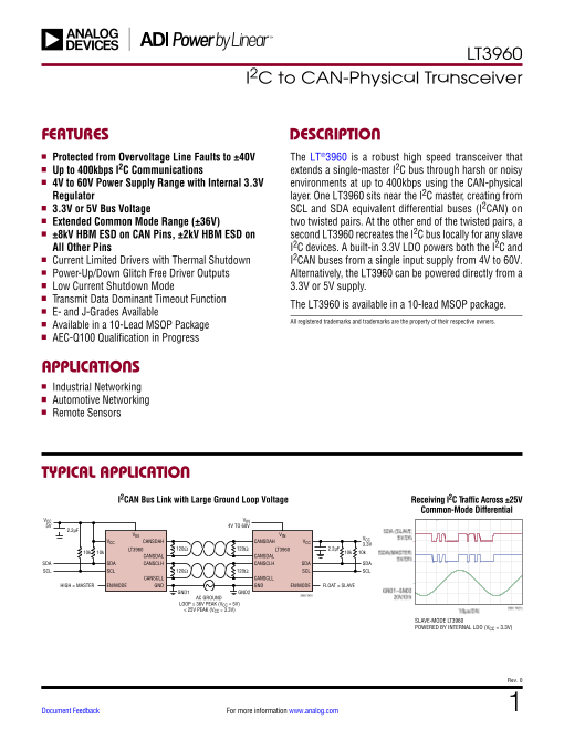
Features、Applications、Typical Application 、Description
LT3960
I2C to CAN-Physical Transceiver
FEATURES DESCRIPTION
n Protected from Overvoltage Line Faults to ±40V The LT®3960 is a robust high speed transceiver that
n Up to 400kbps I2C Communications extends a single-master I2C bus through harsh or noisy
n 4V to 60V Power Supply Range with Internal 3.3V environments at up to 400kbps using the CAN-physical
Regulator layer. One LT3960 sits near the I2C master, creating from
n 3.3V or 5V Bus Voltage SCL and SDA equivalent differential buses (I2CAN) on
n Extended Common Mode Range (±36V) two twisted pairs. At the other end of the twisted pairs, a
n ±8kV HBM ESD on CAN Pins, ±2kV HBM ESD on second LT3960 recreates the I2C bus locally for any slave
All Other Pins I2C devices. A built-in 3.3V LDO powers both the I2C and
n Current Limited Drivers with Thermal Shutdown I2CAN buses from a single input supply from 4V to 60V.
n Power-Up/Down Glitch Free Driver Outputs Alternatively, the LT3960 can be powered directly from a
n Low Current Shutdown Mode 3.3V or 5V supply.
n Transmit Data Dominant Timeout Function The LT3960 is available in a 10-lead MSOP package.
n E- and J-Grades Available
Available in a 10-Lead MSOP Package All registered trademarks and trademarks are the property of their respective owners.
n
n AEC-Q100 Qualification in Progress
APPLICATIONS
n Industrial Networking
n Automotive Networking
n Remote Sensors
TYPICAL APPLICATION
I2CAN Bus Link with Large Ground Loop Voltage Receiving I2C Traffic Across ±25V
Common-Mode Differential
VCC VIN
5V 4V TO 60V
2.2µF SDA (SLAVE)
VIN VIN 5V/DIV
VCC CANSDAH CANSDAH V VCC
CC 3.3V
10k 10k LT3960 120Ω 120Ω LT3960 2.2µF
10k 10k SDA(MASTER)
CANSDAL CANSDAL 5V/DIV
SDA SDA CANSCLH CANSCLH SDA SDA
SCL SCL 120Ω 120Ω SCL SCL
CANSCLL CANSCLL
HIGH = MASTER EN/MODE GND GND EN/MODE FLOAT = SLAVE
GND1 GND2 GND1–GND2
AC GROUND 3960 TA01 20V/DIV
LOOP ≤ 36V PEAK (VCC = 5V)
< 25V PEAK (VCC = 3.3V) 3960 TA01b
10µs/DIV
SLAVE-MODE LT3960
POWERED BY INTERNAL LDO (VCC = 3.3V)
Rev. 0
Document Feedback For more information www.analog.com 1
Page2
Absolute Maximum Ratings、Order Information、Pin Configuration
LT3960
ABSOLUTE MAXIMUM RATINGS PIN CONFIGURATION
(Notes 1, 2, 3)
VIN ............................................................................60V
VCC, EN/MODE .........................................................5.5V TOP VIEW
SDA, SCL .........................................–0.3V to VCC + 0.3V CANSDAL 1 10 SDA
CANSDAH, CANSDAL, CANSCLH, CANSDAH 2
GND 3 11 9 SCL
GND 8 VCC
CANSCLL ................................................ –40V to 40V CANSCLH 4 7 EN/MODE
CANSCLL 5 6 VIN
Operating Junction Temperature Range MSE PACKAGE
LT3960E ............................................ –40°C to 125°C 10-LEAD PLASTIC MSOP
T = 125°C, θ = 40°C/W
LT3960J............................................. –40°C to 150°C JMAX JA
EXPOSED PAD (PIN 11) IS GND, MUST BE SOLDERED TO PCB
Storage Temperature Range .................. –65°C to 150°C
Lead Temperature (Soldering, 10 sec) ................... 300°C
ORDER INFORMATION
LEAD FREE FINISH TAPE AND REEL PART MARKING* PACKAGE DESCRIPTION TEMPERATURE RANGE
LT3960EMSE#PBF LT3960EMSE#TRPBF LHJP 10-Lead Plastic MSOP –40°C to 125°C
LT3960JMSE#PBF LT3960JMSE#TRPBF LHJP 10-Lead Plastic MSOP –40°C to 150°C
AUTOMOTIVE PRODUCTS**
LT3960EMSE#WPBF LT3960EMSE#WTRPBF LHJP 10-Lead Plastic MSOP –40°C to 125°C
LT3960JMSE#WPBF LT3960JMSE#WTRPBF LHJP 10-Lead Plastic MSOP –40°C to 150°C
Contact the factory for parts specified with wider operating temperature ranges. *The temperature grade is identified by a label on the shipping container.
Tape and reel specifications. Some packages are available in 500 unit reels through designated sales channels with #TRMPBF suffix.
**Versions of this part are available with controlled manufacturing to support the quality and reliability requirements of automotive applications. These
models are designated with a #W suffix. Only the automotive grade products shown are available for use in automotive applications. Contact your
local Analog Devices account representative for specific product ordering information and to obtain the specific Automotive Reliability reports for
these models.
Rev. 0
2 For more information www.analog.com
Page3
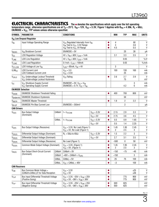
Electrical Characteristics
LT3960
E LECTRICAL CHARACTERISTICS The l denotes the specifications which apply over the full operating
temperature range, otherwise specifications are at TA = 25°C. VIN = 12V, VCC = 3.3V, Figure 1 Applies with RPU = 4.99k, RL = 60Ω,
EN/MODE = VCC, TYP values unless otherwise specified.
SYMBOL PARAMETER CONDITIONS MIN TYP MAX UNITS
VIN Low Dropout Regulator
VIN Input Voltage Operating Range VCC Regulated Internally from VIN l 4 60 V
VIN Tied to VCC, 3.3V Range l 3 3.6 V
VIN Tied to VCC, 5V Range l 4.5 5.5 V
IIN(SD) VIN Shutdown Current EN/MODE = 0V 20 26 µA
VCC LDO Regulation Voltage 4V ≤ VIN ≤ 60V, ILDO = 1mA 3.1 3.3 3.5 V
VLINE LDO Line Regulation 4V ≤ VIN ≤ 60V, ILDO = 1mA 0.05 %/V
VLOAD LDO Load Regulation 0.1mA < ILDO < 100mA 0.05 %/mA
VCC,LOW LDO Voltage at Low VIN ILDO = 85mA, VIN = 4V 3 V
ILIMCC LDO Current Limit VCC = 3.0 100 130 160 mA
LDO Foldback Current Limit VCC = 0.5V 25 mA
VUVLO VCC Undervoltage Lockout Threshold VCC Falling l 2.6 2.7 2.9 V
VCC Undervoltage Lockout Hysteresis 75 mV
ICC VCC Shutdown Supply Current EN/MODE = 0V, VCC = VIN 3 mA
VCC Operating Supply Current EN/MODE ≥ 0.7V, VCC = VIN 4.2 6 mA
EN/MODE Selection
VSHDN EN/MODE Shutdown Threshold Falling l 400 700 800 mV
VSHDN-HYS EN/MODE Shutdown Hysteresis 50 mV
VMSTR EN/MODE Master Threshold l 1.9 2 2.2 V
IEN-UP EN/MODE Pin Bias Current Low EN/MODE = 350mV 2 µA
CAN Drivers
VO(D) Bus Output Voltage CANxH t < tTO:CAN VCC = 3.3V l 2.15 2.9 3.3 V
(Dominant) VCC = 5V l 2.75 3.6 4.5 V
CANxL t < tTO:CAN VCC = 3.3V l 0.5 0.9 1.65 V
VCC = 5V 0.5 1.4 2.25 V
VO(R) Bus Output Voltage (Recessive) VCC = 3.3V, No Load (Figure 1) l 1.45 1.95 2.45 V
VCC = 5V, No Load (Figure 1) l 2 2.5 3 V
VOD(D) Differential Output Voltage (Dominant) RL = 50Ω to 65Ω VCC = 3.3V l 1.5 2.2 3 V
VOD(D) Differential Output Voltage (Dominant) VCC = 5V 2.7 3.1 3.5 V
VOD(R) Differential Output Voltage (Recessive) No Load (Figure 1) l –500 0 50 mV
VOC(R) Common Mode Output Voltage (Dominant) VCC = 3.3V, (Figure 1) l 1.45 1.95 2.45 V
VCC = 5V, (Figure 1) l 2 2.5 3 V
IOS(D) Bus Output Short-Circuit Current CANxH CANxH = 0V l –150 –75 –40 mA
(Dominant) CANxH –40V < CANxH < VO(R) l –150 3 mA
CANxL CANxL = 5V l 25 75 100 mA
CANxL VCC < CANxL < 40V l –3 100 mA
CAN Receivers
VCM Bus Common Mode Voltage = VCC = 3.3V l ±25 V
(CANxH+CANxL)/2 for Data Reception VCC = 5V l ±36 V
VTH+ Bus Input Differential Threshold Voltage VCC = 3.3V, –25V ≤ VCM ≤ 25V l 775 900 mV
(Positive Going) VCC = 5V, –36V ≤ VCM ≤ 36V l 775 900 mV
VTH– Bus Input Differential Threshold Voltage VCC = 3.3V, –25V ≤ VCM ≤ 25V l 500 625 mV
(Negative Going) VCC = 5V, –36V ≤ VCM ≤ 36V l 500 625 mV
Rev. 0
For more information www.analog.com 3
Page4
LT3960
ELECTRICAL CHARACTERISTICS The l denotes the specifications which apply over the full operating
temperature range, otherwise specifications are at TA = 25°C. VIN = 12V, VCC = 3.3V, Figure 1 applies with RPU = 4.99k, RL = 60Ω,
EN/MODE = VCC, TYP values unless otherwise specified.
SYMBOL PARAMETER CONDITIONS MIN TYP MAX UNITS
∆VTH Bus Input Differential Hysteresis Voltage VCC = 3.3V, –25V ≤ VCM ≤ 25V 150 mV
VCC = 5V, –36V ≤ VCM ≤ 36V 150 mV
RIN Input Resistance (CANxH and CANxL) SCL = SDA = VCC; RIN = ∆V/∆I; ∆I = ±20 µA l 25 35.7 50 kΩ
RID Differential Input Resistance SCL = SDA = VCC; RIN = ∆V/∆I; ∆I = ±20 µA l 50 71.4 100 kΩ
∆RIN Input Resistance Matching RIN (CANxH) to RIN (CANxL) l ±3 %
CIH Input Capacitance to GND (CANxH) (Note 4) 32 pF
CIL Input Capacitance to GND (CANxL) (Note 4) 8 pF
CID Differential Input Capacitance (Note 4) 8.4 pF
IL Bus Leakage Current (Power Off) VCC = 0V, CANxH = CANxL = 5V ±10 µA
VCC = 0V, CANxH = CANxL = 5V, t < 150°C l ±50 µA
I2C Port
VIL SDA, SCL Input Low Voltage l 0.4 V
VIH SDA, SCL Input High Voltage l 1.5 V
Ii SDA, SCL Input Leakage Current SDA = SCL = 0V to 5.5V –50 50 nA
Vhys SDA, SCL Input Hysteresis l 0.05 • VCC V
VOL1 SDA, SCL Output Low Voltage ISDA = 3mA l 0.4 V
tr Clock/Data Rise Time CB = Capacitance of One Bus Line (pF) (Note 5) 20 + 0.1CB 300 ns
tf Clock/Data Fall Time CB = Capacitance of One Bus Line (pF) (Note 5) 20 + 0.1CB 300 ns
Rev. 0
4 For more information www.analog.com
Page5
Switching Characteristics
LT3960
S WITCHING CHARACTERISTICS The l denotes the specifications which apply over the full operating
temperature range, otherwise specifications are at TA = 25°C. VIN = 12V, VCC = 3.3V, Figure 2 applies with RPU = 4.99k, RL = 60Ω,
EN/MODE = VCC, TYP values unless otherwise specified.
SYMBOL PARAMETER CONDITIONS MIN TYP MAX UNITS
Transceiver Timing
fSCL SCL Clock Frequency (Notes 5,6) l 0 400 kHz
t I2C to I2PI2CBD CAN Dominant Propagation Delay (Figure 2, Figure 3) VCC = 3.3V l 45 80 130 ns
VCC = 5V l 45 75 115 ns
t I2C to I2PI2CBR CAN Recessive Propagation Delay (Figure 2, Figure 3) VCC = 3.3V l 80 120 170 ns
VCC = 5V l 60 90 120 ns
t 2
PBI2CD I CAN Dominant to I2C Propagation Delay (Figure 2, Figure 3) VCC = 3.3V l 25 40 65 ns
VCC = 5V l 25 40 65 ns
t 2
PBI2CR I CAN Recessive to I2C Propagation Delay (Figure 2, Figure 3) VCC = 3.3V l 25 45 80 ns
VCC = 5V l 20 35 60 ns
t 2
TO;CAN I CAN Dominant Timeout Time (Figure 2, Figure 4) l 0.5 1.5 2 ms
t 2
EN;I2C I C Driver Enable from Shutdown VCC = 3.3V or 5V (Figure 2, Figure 5) l 40 µs
t 2
EN;CAN I CAN Driver Enable from Shutdown VCC = 3.3V or 5V (Figure 2, Figure 6) l 40 µs
t 2
SHDN;I2C Time to Shutdown, I C (Figure 2, Figure 5) l 500 ns
tSHDN;CAN Time to Shutdown, I2CAN (Figure 2, Figure 6) l 500 ns
Note 1: Stresses beyond those listed under Absolute Maximum Ratings Note 3: The LT3960 includes overtemperature protection that is intended
may cause permanent damage to the device. Exposure to any Absolute to protect the device during momentary overload conditions. Junction
Maximum Rating condition for extended periods may affect device temperature will exceed the maximum operating junction temperature
reliability and lifetime. when overtemperature is active. Continuous operating above the specified
Note 2: The LT3960E is guaranteed to meet specified performance maximum operating junction temperature may impair device reliability.
from 0°C to 125°C. Specifications over the –40°C to 125°C operating Note 4: Pin capacitance given for reference only and is not tested in
temperature range are assured by design, characterization and correlation production.
with statistical process controls. The LT3960J is guaranteed to meet Note 5: Rise and fall times are measured at 30% and 70% levels.
performance specifications over the full –40°C to 150°C operating Note 6: Maximum SCL clock frequency will be affected by delays through
junction temperature range. High junction temperatures degrade operating the twisted-pair interface and I/O circuitry of other devices on the bus.
lifetimes. Operating lifetime is derated at junction temperatures greater These delays may limit the operation frequency to below the LT3960
than 125°C. maximum specification.
Note 7: The LT3960 does not support clock stretching. SCL should not be
pulled low by slave devices.
Rev. 0
For more information www.analog.com 5
Page6
Typical Performance Characteristics
LT3960
TYPICAL PERFORMANCE CHARACTERISTICS
TA = 25°C, VCC = 3.3V, RPU = 60Ω unless otherwise noted.
Supply Current (I2CAN Dominant) Supply Current (I2CAN Recessive) Supply Current (I2CAN Dominant)
vs VCC vs VCC vs Temperature
70 6.0 70
5.8
65 65
5.6
60 V = 5V
5.4 60 CC
55 5.2 55
5.0
50 4.8 50
V = 3.3V
45 4.6 CC
45
4.4
40 40
4.2
35 4.0 35
3 3.5 4 4.5 5 5.5 3 3.5 4 4.5 5 5.5 –50 –25 0 25 50 75 100 125 150
VCC (V) VCC (V) TEMPERATURE (˚C)
3960 G01 3960 G02 3960 G03
Supply Current (I2CAN Recessive) I2CAN Differential Output Voltage I2CAN Common Mode Voltage
vs Temperature (Dominant) vs Temperature (Dominant) vs Temperature
5.5 3.4 2.7
5.4 2.6
3.2 VCC = 5V
5.3 VCC = 5V 2.5
5.2 3.0 2.4
5.1 2.8 2.3
5.0
VCC = 3.3V 2.2
4.9 2.6 2.1
4.8 2.4 2.0
4.7 VCC = 3.3V 1.9
2.2 VCC = 3.3V
4.6 1.8
4.5 2.0 1.7
–50 –30 –10 10 30 50 70 90 110 130 150 –50 –25 0 25 50 75 100 125 150 –50 –25 0 25 50 75 100 125 150
TEMPERATURE (˚C) TEMPERATURE (˚C) TEMPERATURE (˚C)
3960 G04 3960 G05 3960 G06
CANxH Short-Circuit Current CANxH Short-Circuit Current I2C to CAN Propagation Delay
(Dominant) vs CANxH Voltage (Dominant) vs CANxH Voltage vs Temperature
0 100 70
–10 90
60
–20 80 DOMINANT
–30 70 50
–40 VCC = 5V 60 VCC = 3.3V
40
–50 50
–60 V 30
CC = 3.3V 40 VCC = 5V
–70 30 20
–80 20
10 RECESSIVE
–90 10
–100 0 0
–40 –35 –30 –25 –20 –15 –10 –5 0 5 0 5 10 15 20 25 30 35 40 –50 –25 0 25 50 75 100 125 150
CANXH (V) CANXL (V) TEMPERATURE (˚C)
3960 G07 3960 G08 3960 G09
Rev. 0
6 For more information www.analog.com
ICANXH(D) (mA)
ICC (mA) ICC(D) (mA)
ICANXL(D) (mA) VOD(D) (V) ICC(R) (mA)
TPI2CB (ns) VOC(D) (V) ICC(D) (mA)
Page7
LT3960
TYPICAL PERFORMANCE CHARACTERISTICS
TA = 25°C, VCC = 3.3V, RPU = 60Ω unless otherwise noted.
CAN to I2C Recessive Propagation EN/MODE Shutdown Thresholds EN/MODE Current vs Temperature
vs Temperature vs Temperature (VCC = 3.3V, 5V) (VEN/MODE = 0.35V)
120 900 2.6
850
2.5
110 800
DOMINANT
750 RISING 2.4
100 700 2.3
650 FALLING
90 2.2
600
80 RECESSIVE 550 2.1
500 2.0
70 450
1.9
400
60 350 1.8
–50 –25 0 25 50 75 100 125 150 –50 –25 0 25 50 75 100 125 150 –50 –25 0 25 50 75 100 125 150
TEMPERATURE (˚C) TEMPERATURE (˚C) TEMPERATURE (˚C)
3960 G10 3960 G11 3960 G12
VIN Shutdown Current VIN Quiescent Current
vs Temperature vs Temperature VCC vs Temperature (Various VIN)
24 220 3.6
VIN = 12V I = 1mA
210 CC
VCC = EN = 5V
22 200 3.5
190
20 180 3.4
170
18 160 3.3
150
16 140 3.2
130
14 120 3.1 VIN = 12V
110 VIN = 24V
VIN = 48V
12 100 3.0
–50 –25 0 25 50 75 100 125 150 –50 –25 0 25 50 75 100 125 150 –50 –25 0 25 50 75 100 125 150
TEMPERATURE (˚C) TEMPERATURE (˚C) TEMPERATURE (°C)
3960 G13 3960 G14 3960 G15
VCC vs Current (Various VIN) VCC UVLO vs Temperature VCC Current Limit vs VIN
3.40 2.80 160
VIN = 5V
3.35 VIN = 12V
V 2.78 140
IN = 24V
3.30 VIN = 48V RISING 120
2.76
3.25 100
2.74
3.20 80
2.72
3.15 60
FALLING
2.70
3.10 40
3.05 2.68 20
3.00 2.66 0
0 15 30 45 60 75 90 105 120 135 150 –50 –25 0 25 50 75 100 125 150 0 5 10 15 20 25 30 35 40 45 50 55 60
VCC CURRENT (mA) TEMPERATURE (°C) VIN (V)
3960 G16 3960 G17 3960 G18
Rev. 0
For more information www.analog.com 7
VCC (V) IIN(SD) (μA) TPBI2C (ns)
VCC UVLO (V) IIN(Q) (μA) VSHDN (V)
ILIMCC (mA) VCC (V) IEN–UP (μA)
Page8
Pin Functions、Block Diagram
LT3960
PIN FUNCTIONS
CANSDAL (Pin 1): Low Level CAN Bus Line. Carries the EN/MODE (Pin 7): MODE/Shutdown pin. Tie above 2.5V
I2C data bus. to select master mode, float pin to select slave mode, or
CANSDAH (Pin 2): High Level CAN Bus Line. Carries the pull this pin to ground for low-power shutdown mode.
I2C data bus. VCC (Pin 8): Low Dropout Regulator Output and Device
CANSCLH (Pin 4): High Level CAN Bus Line. Carries the Power Supply Input. Bypass this pin with a 2.2µF or
I2C clock bus. greater capacitor to ground. Any bypass capacitors must
be located as close to the pin as possible.
CANSCLL (Pin 5): Low Level CAN Bus Line. Carries the
I2C clock bus. SCL (Pin 9): Clock Input or Output Pin for the I2C Serial
Port. When EN/MODE is 2.5V or above, the SCL pin is
GND (Pin 3 and Exposed Pad): Ground. Solder the an input for the master clock. When EN/MODE is float-
exposed pad and pin directly to the ground plane. ing, the SCL pin is an output for data received on the
V (Pin 6): Input Voltage Supply. This pin is the power CANSCLH/L pins.
IN
supply input to the LDO. It must be locally bypassed with SDA (Pin 10): Data Input and Output Pin for the I2C
a 1µF filter capacitor to GND as close to the pin as possi- Serial Port.
ble. If the LDO function is unused, tie VIN to VCC.
BLOCK DIAGRAM
VIN
4V TO 60V
6
VIN
–
0.5V 3.3V
+ SHUTDOWN
VCC VCC
V 2 8
CC EN/MODE I C MASTER V
7 CC 2.2μF
RPU TX TIMEOUT PREDRIVE
SCL
9 MODE
SELECT
35.7k
+ CANSCLH
4
35.7k CANSCLL
– 5
VCC 1.1k 1.1k
1.95V FOR VCC = 3.3V
+ 2.5V FOR VCC = 5V
SHUTDOWN
–
VCC VCC
1.1k 1.1k
RPU TX TIMEOUT PREDRIVE
10 SDA
READ/WRITE 35.7k
ARBITRATION + CANSDAH
2
35.7k CANSDAL
11 – 1
3 GND
3960 BD
Rev. 0
8 For more information www.analog.com
+
–
Page9
Test Circuits
LT3960
TEST CIRCUITS
VCC
5V
1µF VIN CANSDAH
RL/2
CANSDAH 30.1Ω
EN/MODE 1%
VCC VCC CM
R SDA
RPU RPU 2.2µF CANSDAL L/2
30.1Ω
4.99k 4.99k 1%
SDA SDA CANSDAL
LT3960
CANSCLH
RL/2
CANSCLH 30.1Ω
SCL SCL 1%
CM
R SCL
CANSCLL L/2
30.1Ω
1%
GND CANSCLL
3960 F01
Figure 1. All Electrical Characteristic Measurements
VCC
5V
1µF VIN CANSDAH
RL/2
EN/MODE CANSDAH 30.1Ω
1% C
V L
CC VCC CM
R SDA 100pF
RPU RPU 2.2µF CANSDAL L/2
30.1Ω 4.7nF
1k 1k 1%
SDA SDA CANSDAL
LT3960
15pF CANSCLH
RL/2
CANSCLH 30.1Ω
SCL SCL 1%
CM CL
R SCL
15pF 100pF
CANSCLL L/2
30.1Ω 4.7nF
1%
GND CANSCLL
3960 F02
Figure 2. All Switching Characteristic Measurements
Rev. 0
For more information www.analog.com 9
Page10
Timing Diagrams
LT3960
TIMING DIAGRAMS
HIGH
SCL (MASTER) 0.7VDD
0.3VDD LOW
CANSCLH HIGH
SCL (MASTER) 0.3VDD LOW
CANSCLL
CANSCLH
DOMINANT
V CANSCLL
OD 0.9V
0.5V
RECESSIVE DOMINANT
HIGH V 0.9V
SCL (SLAVE) 0.7V OD
0.3V DD
DD 0.5V
LOW RECESSIVE
tPI2CBD tPI2CBR tTO;CAN
t 3960 F04
PBI2CD tPBI2CR 3960 F03
Figure 3. Transceiver Data Propagation Timing Diagram Figure 4. I2CAN Dominant Timeout
1.2V (SLAVE MODE) 2.5V (MASTER MODE)
EN 0.75V 0.7V EN 0.75V 0.7V
SCL OR SDA 0.7VCC
0.3V SCL OR SDA
DD 0.3VDD
tEN;I2C tSHDN;I2C tEN;CAN tSHDN;CAN
CANxH CANxH CAN
CANxL CANxL
V 0.9V V 0.9V
OD OD
0.5V 0.5V
3960 F05 3960 F06
Figure 5. I2CAN Enable and Disable Times Figure 6. I2CAN Enable and Disable Times
Rev. 0
10 For more information www.analog.com
Page11
Operation
LT3960
OPERATION
The LT3960 is a high-speed transceiver which creates the the VCC pin from which the transceivers and bus lines are
functional equivalent of a single-master I2C bus in the CAN powered. Alternatively, the LT3960 can by powered from
physical layer and is powered from a single wide-ranging a supply voltage of 3.3V or 5V on VIN, bypassing the LDO
input voltage. Using two integrated CAN transceivers, the by shorting VCC to VIN.
LT3960 creates a differential proxy for each of the sin-
2 The EN/MODE pin is used to put the LT3960 in low power
gle-ended I C clock and data signals which is capable shutdown mode and selects between Master and Slave
of traversing harsh or noisy environments across two modes of operation when enabled. When the EN/MODE
twisted pairs. pin is below 0.7V, (typical) the LT3960 is in shutdown
Each transceiver consists of a transmitter and receiver, mode, disabling both the LDO and transceivers. When
capable of quickly converting a single-ended I2C domi- VIN is powered, floating the EN/MODE pin or driving it
nant signal into a differential dominant signal, and vice between 0.7V and 2.0V (typical) enables the LDO and
versa. The transmitter is a current-regulated differential sets the transceiver in Slave Mode. An EN/MODE voltage
driver that generates a differential voltage between the above 2.0V (typical) with VIN is powered sets the LT3960
CANxH and CANxL pins determined by drive current and in Master Mode.
the equivalent resistive load on the CANx bus. Common- Bidirectional communication is supported on the data
mode voltage of the CANx bus is regulated by the trans- channel (SDA and CANSDA) regardless of the mode of
mitter when driving dominant as described in the applica- operation. Communication on the clock channel (SCL
tions section. The receiver is a CAN compatible differential and CANSCL) is unidirectional, with the direction deter-
receiver with a wide common-mode range of ±25V or mined by the selected mode of operation. In Slave Mode,
±36V, depending on VCC voltage. an LT3960 only communicates clock signals from the
In the simplest setup, two LT3960 devices are used CANSCL bus to the SCL bus. Any LT3960 connected to
(Figure 7). The first is connected to the I2C master (micro- slave I2C devices should be operated in Slave Mode. In
controller or otherwise). The second LT3960 is connected Master Mode, an LT3960 only communicates clock sig-
to the first by two twisted pairs and regenerates the I2C nals from the SCL bus to the CANSCL bus. The LT3960
bus locally for one or more I2C slave devices. The LT3960 connected to the I2C master device should always be
devices transmit the clock signal in only one direction, operated in Master Mode. Regardless of the number of
from master to slave. Bidirectional communication of the LT3960 devices tied to a I2CAN bus in a given applica-
data signal is always permitted. tion, exactly one will operate in Master Mode, driving the
The LT3960 contains an integrated LDO which regulates clock signal to the I2CAN bus and, ultimately, to all I2C
an input from the V pin between 4V and 60V to 3.3V on slave devices. The LT3960 does not support multi-master
IN I2C systems.
CIRCUIT BOARD 1 CIRCUIT BOARD 2
3.3V OR 5V 4V TO 60V
VIN VIN
VCC CANSDAH CANSDAH EN/MODE
µCONTROLLER LT3960 LT3960 VCC
CANSDAL CANSDAL I2C
SDA SDA CANSCLH CANSCLH SLAVE
SCL SCL SDA SDA
DIG I/O EN/MODE CANSCLL CANSCLL SCL SCL
GND GND
3960 F07
Figure 7. Simple Single-Slave Application
Rev. 0
For more information www.analog.com 11
Page12
LT3960
OPERATION
Data Transmission Detail CANSDA bus. The primary factor determining the direction
The timing diagram in Figure 8 shows how a byte of data of communication is the time of arrival of dominant sig-
is sent by the I2C master and acknowledged by the I2C nals on SDA and CANSDA. The first of SDA and CANSDA
slave in the single-master single-slave system described to be asserted dominant by an external device will cause
in Figure 7. The I2C master issues a start command to the LT3960 to drive the other dominant, establishing the
initiate a communication frame. The LT3960 connected to direction of communication until it is released and returns
the master drives the CANSCL and CANSDA buses dom- to a recessive state. The transmitter which opposes the
inant in response to the change in state on the SCL and established direction of communication will be blocked
SDA pins without interpretation or delay. The LT3960 con- until it can be safely re-enabled without locking up a bus
nected to the I2C slave receives the dominant signals on or misinterpreting the direction of communication. To
the CANSCL and CANSDA buses and drives the slave SCL fully describe the method of arbitration, communication
and SDA pins dominant without interpretation or delay. in each direction is described in detail below.
The result on the slave I2C bus is an I2C Start command In the default state, SDA and CANSDA are in a recessive
nearly identical to that generated by the master, delayed by state and no direction of communication is set. If SDA is
propagation delays of the master LT3960, twisted pairs, asserted dominant (low) by an external I2C device from
and slave LT3960. a default state, the LT3960 will drive CANSDA dominant
As additional clock and data edges are written by the I2C and the LT3960’s receiver on CANSDA is blocked from
master, they too are recreated, first on the CANSCL and driving SDA. When the SDA line is eventually released by
CANSDA buses and then on the slave I2C bus. Once the the external I2C device and returns to a recessive state,
entire byte of data is written on the slave I2C bus, the I2C the LT3960 stops driving the CANSDA bus dominant.
slave device issues an ACK, pulling down SDA to acknowl- After allowing the CANSDA bus sufficient time to return
edge receipt of a valid byte. The slave LT3960 recognizes to a passive state as required by the CAN physical layer
that a slave I2C device is driving the SDA line dominant specifications, the LT3960 reopens the possibility of bidi-
and switches from receiving to transmitting to drive the rectional traffic and waits for a dominant signal on SDA or
CANSDA bus dominant. The master LT3960 then receives CANSDA to once again set a direction for communication.
the ACK on the CANSDA bus and pulls the master SDA If, from the default state, CANSDA is asserted dominant
low, communicating the ACK to the master. by another LT3960 on the bus while SDA remains reces-
Note that clock data is always transmitted from master to sive (high), the LT3960 will drive SDA dominant (low)
slave, but the LT3960 dynamically switches the direction and the CAN transmitter is blocked from driving CANSDA
of SDA communication based primarily on the time of based on its input while CANSDA is held dominant. When
arrival of dominant signals on its inputs. the CANSDA bus returns to a recessive state, the LT3960
stops driving the other dominant. When it is safe to do so
Bidirectional Arbitration of SDA without causing glitches or latch up, the LT3960 reopens
The LT3960 facilitates bidirectional SDA communication the possibility of bidirectional traffic and waits for a dom-
between master and slave I2C devices by dynamically inant signal on SDA or CANSDA to once again set a direc-
controlling the direction of traffic between SDA and the tion for communication.
Rev. 0
12 For more information www.analog.com
Page13
LT3960
OPERATION
I2C START I2C STOP
SCL (MASTER)
SDA (MASTER) 1 1 0 0 1 1 0 0 ACK
MASTER
LT3960
CANSCL
CANSDA ACK
TWISTED PAIRS
CANSDA ACK
CANSCL
SLAVE
LT3960
I2C START I2C STOP
SCL (SLAVE)
SDA (SLAVE) 1 1 0 0 1 1 0 0
3960 F08
ACK FROM I2C SLAVE
Figure 8. Simple Single-Slave Application
Rev. 0
For more information www.analog.com 13
Page14
Applications Information
LT3960
APPLICATIONS INFORMATION
Supply Voltage Ranges 3.3V OR 5V
BUS VOLTAGE
The LT3960 can be operated with or without using its VCC VIN
2.2µF V
internal LDO. Tying VIN to VCC and powering directly from 30k CC
LT3960
µCONTROLLER
a 3.3V or 5V supply will bypass the LDO. With a 5V supply EN/MODE
on VCC, transmitter common-mode voltage and receiver I/O EN
common-mode input range are increased from their 3.3V 3960 F09
values. In this configuration, an internal comparator mon-
itors the supply voltage and switches internal reference Figure 9. Recommended Master Mode Power Setup
voltages and output drive strengths at approximately An LT3960 connected to slave I2C devices must be oper-
4.1V. Operation with a supply between 3.6V and 4.5V is ated in Slave Mode, with the EN/MODE pin between 0.7V
not recommended, because of the discontinuity in the and 2V. When left floating, the EN/MODE pin will pull
internal voltages at this switch point. up to approximately 1.2V, enabling the LT3960 and set-
When using the internal LDO to generate the 3.3V bus ting it in Slave Mode, whenever the VIN pin is powered
supply on VCC, any VIN supply voltage between 4V and above approximately 2V. It is recommended that the EN/
60V is allowed. In this configuration, the switch point MODE pin be left floating for Slave Mode LT3960 devices,
mentioned above is avoided since VCC is regulated to a regardless of whether the internal LDO is employed.
fixed 3.3V. LT3960 and Standard CAN Transceivers
An LT3960 operating with a VCC at 5V may share an I2CAN
bus with an LT3960 operating with V at 3.3V. However, It should be noted that while the LT3960 uses the CAN
CC 2
the fluctuation in common mode voltage between 1.95V physical layer to conduct bidirectional I C data, the
(when an LT3960 with VCC = 3.3V is dominant) and CANSCL and CANSDA buses created by the LT3960 are
2.5V (when an LT3960 with V = 5V is dominant) may not traditional CAN buses carrying traditional CAN data. As
CC
increase electromagnetic emissions. such, the CANSCL and CANSDA buses between LT3960
devices cannot be shared with standard CAN transceivers
Master and Slave Mode Configurations in a multidrop configuration.
The LT3960 connected to the I2C master must be oper- ±40V Fault Protection
ated in Master Mode, with the EN/MODE pin driven greater
than 2.5V. When operating in Master Mode, it is recom- The LT3960 provides ±40V fault protection on the
2
mended that VCC be tied to V and driven from a bus I CAN interface pins (CANSCLH, CANSCLL, CANSDAH,
IN 2
voltage of 3.3V or 5V. Additionally, EN/MODE should be CANSDAL), allowing I C communication in applications
driven from a digital output pin from the I2C Master as where it was previously impractical. Addressing the need
shown below. In this configuration, EN/MODE can be held the overvoltage tolerance in many industrial and auto-
low until the V cap is fully charged. motive applications, the driver outputs use a progressive
CC foldback current limit to protect against overvoltage faults
Do not tie the EN/MODE pin directly to VCC when oper- while still allowing high current output drive. The LT3960
ating in Master Mode. With EN/MODE and VCC shorted, is protected from ±40V faults powered or unpowered,
every power-up sequence will set the LT3960 into slave even in the case of VCC open or shorted to ground. When
mode for many microseconds while the VCC capacitor VCC is open or shorted to GND, the transceivers are off and
charges between the enable threshold and the Master the I2CAN bus pins remain in the high impedance state.
Mode threshold.
Rev. 0
14 For more information www.analog.com
Page15
LT3960
APPLICATIONS INFORMATION
±8kV ESD Protection in the dominant state. For example, if the SCL line is held
The LT3960 features robust ESD protection. All I2CAN low in Master Mode, a dominant state is asserted on the
interface pins (CANSCLH, CANSCLL, CANSDAH, CANSCL bus until the timer expires, after which the driver
CANSDAL) are protected to ±8kV HBM with respect to releases the bus to a recessive state. The timer is reset
GND, powered or unpowered and all other pins are pro- when SCL is brought high.
tected to 2kV HBM to ensure reliable operation in severe I2CAN Driver Overvoltage, Overcurrent, and
environmental conditions. For applications where greater Overtemperature Protection
ESD protection of interface pins is needed, a simple net-
work providing IEC 61000-4-2 Level 4 ESD protection is The I2CAN driver outputs are protected from short cir-
shown in the Typical Application section. cuits to any voltage within the absolute maximum range
of -40V to 40V. The maximum current on I2CAN interface
±36V Extended Common-Mode Range pins in a fault condition is ±150mA. The drivers include a
The LT3960 receiver features an extended common progressive foldback current limiting circuit that contin-
mode range of -36V to 36V when operating from a 5V uously reduces the driver current with increasing output
V and -25V to 25V when operating from a 3.3V V . fault voltage. The fault current is typically ±2mA for faults
CC CC
The wide common mode increases the reliability of oper- at the absolute maximum voltages of ±40V.
ation in environments with electrical noise or local ground The LT3960 also features thermal shutdown protection
potential differences due to ground loops. This extended that disables the chip in the case of excessive power
common mode range allows the LT3960 to conduct I2C dissipation from the drivers. When the die temperature
communication in environments inhospitable to standard exceeds 168 ˚ C (typical), the LT3960 is forced into shut-
I2C, such as between two distant PCBs in an automobile. down mode and the I2CAN drivers enter a high impedance
state.
I2CAN Driver
When the SCL or SDA pin is asserted low by external Power-Up/Down Glitch-Free Outputs
I2C device and the conditions are met (whether by mode The LT3960 employs an undervoltage monitoring circuit
selection or bidirectional arbitration) to propagate this on the VCC supply to control the activation of the trans-
data from I2C to CAN, the I2CAN driver asserts the dom- ceiver circuitry. During start-up SDA, SCL, and all I2CAN
inant state on the corresponding bus lines; the CANxH outputs are in a high impedance state until VCC reaches a
driver pulls high and the CANxL driver pulls low. When the voltage sufficient to reliably operate the chip. At this point,
SCL or SDA pin is high under these same conditions, the if EN/MODE is out of its shutdown region, the chip acti-
I2CAN driver is in the recessive state; both the CANxH and vates. The CANSCL and CANSDA receivers activate after
CANxL drivers are in the high impedance state and the bus a short delay tEN;I2C allowing SCL or SDA to follow the
termination resistor equalizes the voltage on CANxH and state of CANSCL or CANSDA. The CANSCL and CANSDA
CANxL. In the recessive state, the impedance on CANxH drivers power up in the transmit dominant timeout state
and CANxL is determined by the receiver input resistance, regardless of the state of SCL or SDA and remain in the
RIN. When EN/MODE is low or the VCC is in UVLO, the recessive state until the first high to low transition of SCL
LT3960 is in shutdown; all I2CAN drivers are in the high or SDA, respectively. This assures that the LT3960 does
impedance state, and the receiver input resistance RIN is not disturb the I2CAN bus by glitching to the dominant
disconnected from the bus by a FET switch. state during start-up.
Transmit Dominant Timeout Function During power-down, similar protection exists. When the
undervoltage detection circuit senses low supply voltage
Both transceivers in the LT3960 include a 1.5ms (typical) on VCC, it immediately puts the chip into shutdown. All
timer to limit the time that driver can hold the I2CAN bus I2C and I2CAN pin outputs go the high impedance state.
Rev. 0
For more information www.analog.com 15
Page16
LT3960
APPLICATIONS INFORMATION
Passive Leakage on I2CAN Bus Pins RESISTOR TERMINATION
When the power supply is removed or the chip is in shut- CANxH CANxH BUS
down, the I2CAN pins are in a high impedance state. The LT3960 120Ω
I2CAN receiver inputs are isolated from the CANxH and
CANxL pins by FET switches which open in the absence CANxL CANxL BUS
of power, preventing the resistor dividers on the receiver
inputs from loading the bus. The high impedance state SPLIT TERMINATION
of I2CAN pins is maintained over a range determined by CANxH CANxH BUS
the ESD protection of the pins, typically -0.3V to 7V. For 60Ω
LT3960
bus voltages outside this range, the current flowing into 60Ω 4.7nF
the receiver is governed by the conduction voltages of CANxL CANxL BUS
3960 F10
the ESD device and the 35.7k nominal I2CAN receiver
input resistance. Figure 10. Split Termination for Improved
Common Mode Behavior
I2CAN Bus Termination
VCC = 3.3V
I2
SDA
CAN buses must be terminated at the ends of each 5V/DIV
twisted pair with a 120Ω resistor. Split termination is an CANSDAH
optional termination technique to reduce common mode 1V/DIV
voltage perturbations that can produce EME. A split ter- CANSDAL
1V/DIV
minator divides the single line-end termination resistor CANSDA CM
(nominally 120Ω) into two series resistors of half the 50mV/DIV
value of the single termination resistor (Figure 10). 3960 F11
200ns/DIV
The center point of the two resistors is connected to a Figure 11. I2CAN Common Mode Noise (4.7nF Split Cap)
4.7nF capacitor. Split termination suppresses common
mode voltage perturbations by providing a low impedance VCC = 3.3V
SDA
load to common mode noise sources such as transmitter 5V/DIV
noise or coupling to external noise sources. In the case CANSDAH
1V/DIV
of single resistor termination, the only load on a com-
mon mode noise source is the parallel impedance of the CANSDAL
1V/DIV
input resistors of the I2CAN transceivers on the bus. This CANSDA CM
results in a common mode impedance of several kΩ for a 500mV/DIV
3960 F12
small network. The split termination, on the other hand, 200ns/DIV
provides a common mode load equal to the parallel resis- Figure 12. I2CAN Common Mode Noise (No Split Cap)
tance of the two split termination resistors (30Ω). This
low common mode impedance results in a reduction of
the common mode noise voltage compared to the much
higher common mode impedance of the single resistor
termination. Figure 11 and Figure 12 compare the com-
mon mode noise of an application with and without split
cap termination.
Rev. 0
16 For more information www.analog.com
Page17
LT3960
APPLICATIONS INFORMATION
Multidrop Applications of the propagation delays (tPI2CBD and tPBI2CD), slave ACK
The LT3960 can be used in a multidrop setup, employ- time (tVD;ACK), and master data setup time (tSU;ACK). This
ing multiple slave-mode LT3960’s to generate multiple requirement is shown explicitly in Equation 1.
local I2C buses on multiple PCBs along the length of the tLOW >2(tPI2CBD,max + tCABLE + tPBI2CD,max )
I2CAN bus lines. No additional termination is required in +t (1)
VD;ACK,max + tSU;ACK
a multidrop system, but some care must be taken in the
design of such systems. The stub length, or the distance A conservative estimate of propagation delay
from twisted pairs to any additional LT3960, should be through a twisted pair based on cable length is shown in
less than 0.3m. Stub lengths to the CANSDA and CANSCL Equation 2. Equation 2 is useful for rough estimates, but
buses should be as close as possible in length to avoid when designing applications always calculate propaga-
adding unequal transmission delays to the clock and tion delay based on the actual physical properties of the
data signals. cabling used for the I2CAN bus lines.
120Ω 120Ω
t = ICABLE
CABLE (2)
0.15m/ns
I2C SLAVE LT3960
Fast-mode (400kHz capable) I2C devices are allowed 0.9µs
to acknowledge a valid data byte, even while ACK times
(tVD;ACK) are often much shorter in practice. A tVD;ACK of
0.9µs would limit the data transmission rate of a LT3960
I2C SLAVE LT3960 application to under 400kHz for even one meter of twisted
pair. For this reason, it is recommended that all I2C slaves
be Fast-mode Plus (1MHz) devices instead of Fast-mode
(400kHz) devices when attempting to maximize trans-
I2C SLAVE
LT3960 mission rate. The shorter maximum tVD;ACK (450ns) of
I2C SLAVE Fast-mode plus devices allows for communication across
120Ω 120Ω
3960 F14 a greater distance at any given clock speed. Figure 14
consolidates the information above, plotting maximum
Figure 13. Multidrop Setup clock speeds for a given bus length for applications with
Maximum Data Transmission Rate fast-mode and fast-mode plus devices.
Successful communication in any I2C application is 450
dependent on slave I2C devices’ timely acknowledgment 425
(or ACK) upon receiving a byte of data. Specifically, I2C 400
slaves must assert the SDA line after the eighth clock 375
pulse leaving enough setup time before the ninth rising 350
edge of SCL to guarantee that the ACK will be received by 325
the I2C master. This requirement is straightforward when 300
275
all I2C devices share the same I2C bus, but in LT3960
250
applications where master and slave I2C buses are sepa-
225 FAST–MODE SLAVE DEVICES
rated by various propagation delays, extra care must be FAST–MODE PLUS SLAVE DEVICES
200
taken to ensure that ACKs from slave I2C devices will be 0 5 10 15 20 25 30 35 40 45 50
received by the I2C master at the desired transmission BUS LENGTH (m)
3960 F14
rate. In LT3960 applications, the SCL low period between
successive clock pulses (tLOW)must be less than the sum Figure 14. Maximum I2CAN Clock Speed
Rev. 0
For more information www.analog.com 17
MAX CLOCK SPEED (kHz)
Page18
Typical Applications
LT3960
TYPICAL APPLICATIONS
1A Matrix LED Dimmer with Remote I2C Control
31V TO 36V
(ENABLED AT 33V,
SHUTDOWN AT 31V) LED1+
VIN1 BST1
10µF 2.2µF 0.22µF
×2 50V 68µH 100mΩ LED1+
50V 100k GND SW1 DRN8 VIN 31V TO 36V
1MΩ 100nF 10k 1µF
50V 50V
EN/UVLO FB1 10µF SRC8 ENH
DRN7
3.92k 274k 31.6k 49.9k
LT3964
SRC7 LT3967
+
INTV DRN6 LED1
INTV CC INTV
CC VDD CC
INTVCC ISP1 SRC6 1µF
2.2µF PWM1 ISN1 DRN5 GND 100k
INTVCC
CTRL1 SRC5 ALERT ALERT
PWMTG1 DRN4
ADDR1 499k ADDR4 INTVCC
ADDR-1100011 ADDR3 ADDR-0101100
ADDR2 TSET SRC4 ADDR2
DRN3 ADDR1 POR-LED OFF
SYNC/CLKOUT CLOCK 165k UP TO 26V LED 22k
ALERT ALERT SRC3 RTCLK CLOCK
DRN2
SCL RT WDI 28k (FROM
178k SRC2 10nF LT3964)
SDA GND 360kHz DRN1
SCL
SRC1 SDA
2-WIRE I2C INTERFACE
1µF
3.3V
OR 5V 2.2µF VIN VIN
V CANSDAH CANSDAH V
μCONTROLLER CC CC
I2C MASTER LT3960 120Ω 120Ω LT3960 2.2µF
5k 5k 10k 10k
CANSDAL CANSDAL
SDA SDA CANSCLH CANSCLH SDA
SCL SCL 120Ω 120Ω SCL
DIG I/O EN/MODE CANSCLL CANSCLL EN/MODE
GND GND GND
3960 TA03
GND1 GND2
REMOTE I2C MASTER
Rev. 0
18 For more information www.analog.com
Page19
LT3960
PACKAGE DESCRIPTION
MSE Package
10-Lead Plastic MSOP, Exposed Die Pad
(Reference LTC DWG # 05-08-1664 Rev I)
BOTTOM VIEW OF
EXPOSED PAD OPTION
1.88 ±0.102 1.88
(.074 ±.004) 0.889 ±0.127 1 (.074) 0.29
(.035 ±.005) 1.68 REF
(.066)
5.10 0.05 REF
(.201) 1.68 ±0.102 3.20 – 3.45
MIN (.066 ±.004) (.126 – .136) DETAIL “B”
CORNER TAIL IS PART OF
DETAIL “B” THE LEADFRAME FEATURE.
10 FOR REFERENCE ONLY
0.50 NO MEASUREMENT PURPOSE
0.305 ± 0.038 (.0197) 3.00 ±0.102
(.0120 ±.0015) BSC (.118 ±.004)
TYP 0.497 ±0.076
(NOTE 3) (.0196 ±.003)
RECOMMENDED SOLDER PAD LAYOUT 10 9 8 7 6
REF
4.90 ±0.152 3.00 ±0.102
(.193 ±.006) (.118 ±.004)
DETAIL “A” (NOTE 4)
0.254
(.010) 0° – 6° TYP
GAUGE PLANE 1 2 3 4 5
0.53 ±0.152 1.10 0.86
(.021 ±.006) (.043) (.034)
MAX REF
DETAIL “A”
0.18
(.007) SEATING
PLANE 0.17 – 0.27 0.1016 ±0.0508
(.007 – .011)
0.50 (.004 ±.002)
TYP
(.0197) MSOP (MSE) 0213 REV I
NOTE:
1. DIMENSIONS IN MILLIMETER/(INCH) BSC
2. DRAWING NOT TO SCALE
3. DIMENSION DOES NOT INCLUDE MOLD FLASH, PROTRUSIONS OR GATE BURRS.
MOLD FLASH, PROTRUSIONS OR GATE BURRS SHALL NOT EXCEED 0.152mm (.006") PER SIDE
4. DIMENSION DOES NOT INCLUDE INTERLEAD FLASH OR PROTRUSIONS.
INTERLEAD FLASH OR PROTRUSIONS SHALL NOT EXCEED 0.152mm (.006") PER SIDE
5. LEAD COPLANARITY (BOTTOM OF LEADS AFTER FORMING) SHALL BE 0.102mm (.004") MAX
6. EXPOSED PAD DIMENSION DOES INCLUDE MOLD FLASH. MOLD FLASH ON E-PAD
SHALL NOT EXCEED 0.254mm (.010") PER SIDE.
Rev. 0
Information furnished by Analog Devices is believed to be accurate and reliable. However, no responsibility is assumed by Analog
Devices for its use, nor for any infringements of patents or other rights of third parties that may result from its use. Specifications
subject to change without notice. No license Fiso gr rmanoterde biny fiomrpmlicaattiion owr wotwhe.arwniasleo ugn.cdeorm any patent or patent rights of Analog Devices. 19
Page20
Typical Application、Related Parts
LT3960
TYPICAL APPLICATION
Network for IEC 6100-4-2 Level 4 ESD Protection
CANSDAL CANSDAL
60.4Ω CANSDAH
4.7nF
60.4Ω TVS
CANSDAH
GND GND LT3960
CANSCLH
60.4Ω TVS
4.7nF
60.4Ω CANSCLH
CANSCLL CANSCLL
3960 TA02
TVS: ON SEMI NUP2105L, 350W DUAL BIDIRECTIONAL TVS DIODE, SOT-23
RELATED PARTS
PART NUMBER DESCRIPTION COMMENTS
LT3965 8-Switch Matrix LED Dimmer I2C Multidrop Serial Interface, 16 Unique I2C Addresses, VDD Range: 2.7V to 5.5V,
VIN Range: 8V to 60V, Digital Programmable 256:1 PWM Dimming, 28-Lead TSSOP
LT3967 1.3A Eight-Switch Matrix LED Controls LED Dimming of Strings Up to 54V, I2C Serial Interface with Programmable
Dimmer with CRC-8 Address, 28-Lead TSSOP
LT3964 Dual 36V Synchronous 1.6A Buck Wide Input Voltage Range: 4V to 36V, Two Independent 1.6A/40V Synchronous Bucks,
LED Driver with I2C I2C Interface for Internal True Color PWM™ Dimming (8192:1), 36-Lead QFN
LTC4331 I2C Slave Device Extender Over Up to 1MHz Serial Clock, Fast-Mode Plus (FM+), Selectable Link Baud Rates Extend I2C
Rugged Differential Link Up to 1200m, 20-Lead QFN
Rev. 0
10/20
20 www.analog.com
For more information www.analog.com ANALOG DEVICES, INC. 2020