


データ転送速度の限界を打ち破るフラグシップ・デジタイザ・カードM5i.33xx-x16シリーズ
カード概略仕様
PCIe x16 Gen3 1 Channel 2 Channels Bandwidth
M5i.3337-x16 6.4 GS/s 3.2 GS/s 2 GHz
M5i.3330-x16 6.4 GS/s --- 2 GHz
M5i.3357-x16 10 GS/s 5 GS/s 3 GHz
M5i.3350-x16 10 GS/s --- 3 GHz
このカタログについて
| ドキュメント名 | データ転送速度の限界を打ち破るフラグシップ・デジタイザ・カードM5i.33xx-x16シリーズ |
|---|---|
| ドキュメント種別 | 製品カタログ |
| ファイルサイズ | 715.2Kb |
| 登録カテゴリ | |
| 取り扱い企業 | 株式会社エレクトロニカ IMT事業部 (この企業の取り扱いカタログ一覧) |
この企業の関連カタログ


このカタログの内容
Page1
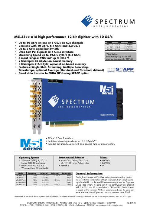
M5i.33xx-x16 high performance 12 bit digitizer with 10 GS/s、General Information
M5i.33xx-x16 high performance 12 bit digitizer with 10 GS/s
• Up to 10 GS/s on one or 5 GS/s on two channels Speed SNR ENOB
• Versions with 10 GS/s, 6.4 GS/s and 3.2 GS/s 10.0 GS/s 52.3 dB 8.3 ENOB
6.4 GS/s 54.0 dB 8.7 ENOB
• Up to 3 GHz signal bandwidth 3.2 GS/s 54.5 dB 8.8 ENOB
• Ultra Fast PCI Express x16 Gen3 interface
• Streaming Speed up to 12.8 GByte/s (6.4 GS/s) FPGA Option:
• 4 input ranges: ±200 mV up to ±2.5 V Block Average up to 1M with
selective averaging for TOFMS
• 2 GSamples (4 GByte) on-board memory
• 8 GSamples (16 GByte) optional on-board memory
• Features: Single-Shot, Streaming, Multiple Recording,
Timestamps, optional Average (Standard and Threshold defined)
• Direct data transfer to CUDA GPU using SCAPP option
• PCIe x16 Gen 3 Interface
• Sustained streaming mode up to 12.8 GByte/s**
• Included advanced cooling with dual cooling fans for proper airflow
Operating Systems Recommended Software Drivers
• Windows 7 (SP1), 8, 10, 11 • Visual C++, Delphi, GNU C++, • MATLAB
Server 2008 R2 and newer VB.NET, C#, Java, Python, Julia • LabVIEW
• Linux Kernel 3.x, 4.x, 5.x • SBench 6 • IVI
• Windows/Linux 32 and 64 bit
Model Resolution 1 channel 2 channels Bandwidth General Information
M5i.3357-x16 12 Bit 10 GS/s 5.0 GS/s 3 GHz
M5i.3350-x16 12 Bit 10 GS/s 3 GHz The high-performance M5i.33xx series gives outstanding perfor-
M5i.3337-x16 12 Bit 6.4 GS/s 3.2 GS/s 2 GHz mance with the combination of high resolution, high samplingrate,
M5i.3330-x16 12 Bit 6.4 GS/s - 2 GHz high bandwidth and the world fastest streaming speed for Digitizers.
M5i.3321-x16 12 Bit 3.2 GS/s 3.2 GS/s 1 GHz On selected systems the card can stream continuously one channel
with 6.4 GS/s and 12 bit resolution to CPU or GPU. The M5i series
is based on the common API from Spectrum and uses the same soft-
ware interface like all Spectrum products released since 2005.
*Some x16 PCIe slots are for the use of graphic cards only and can’t be used for other cards.**Throughput measured with a PCIe root complex supporting a TLP size of 512 bytes.
SPECTRUM INSTRUMENTATION GMBH · AHRENSFELDER WEG 13-17 · 22927 GROSSHANSDORF · GERMANY 13.3.2023
PHONE: +49 (0)4102-6956-0 · FAX: +49 (0)4102-6956-66 · E-MAIL: info@spec.de · INTERNET: www.spectrum-instrumentation.com
Page2
Software Support
Software Support C/C++ and can easily be implemented, expanded and modified
with normal programming skills.
Windows drivers
The cards are delivered with drivers for Windows 7, Windows 8, Hardware features and options
Windows 10 and Windows 11 (each 32 bit and 64 bit). Program-
ming examples for Visual C++, Delphi, Visual Basic, VB.NET, C#, PCI Express x16
Python, Java, Julia and IVI are included. The M5i series cards use a PCI
Express x16 Gen 3 connection.
Linux Drivers They can be used in PCI Express
All cards are delivered with full Linux support. Pre com- x16 slots with hosts supporting
piled kernel modules are included for the most common Gen1, Gen2, Gen3 or Gen4.
distributions like Fedora, Suse, Ubuntu LTS or Debian. The Gen3 or Gen4 is needed to get full performance. The maximum sus-
Linux support includes SMP systems, 32 bit and 64 bit tained data transfer rate is more than 12.8 GByte/s per slot on sys-
systems, versatile programming examples for GNU C++, tems with a PCIe payload size of 512. Physically supported slots
Python and Julia, as well as the possibility to get the kernel driver that are electrically connected with less lanes can also be used with
sources for your own compilation. the M5i series cards, but with reduced data transfer rates.
Connections
SBench 6
The cards are equipped with SMA connectors for the
A base license of SBench 6, the analog signals as well as for clock input and output,
easy-to-use graphical operating trigger input and four multi-function I/O connectors
software for Spectrum cards, is in- (X0, X1, X2, X3). These multi-function connectors can
cluded in the delivery. The base li- be individually programmed to perform different
cense makes it is possible to test functions:
the card, display acquired data
and make some basic measure- • Trigger output
ments. It's a valuable tool for • Status output (armed, triggered, ready, ...)
checking the card’s performance • Synchronous digital inputs, being stored inside
and assisting with the unit’s initial the analog data samples
setup. The cards also come with a demo license for the SBench 6 • Asynchronous I/O lines
professional version. This license gives the user the opportunity to • Logic trigger inputs
test the additional features of the professional version with their
hardware. The professional version contains several advanced
measurement functions, such as FFTs and X/Y display, import and Input Amplifier
export utilities as well as support for all acquisition modes including The analog inputs can be adapt-
data streaming. Data streaming allows the cards to continuously ac- ed to real world signals using a
quire data and transfer it directly to the PC RAM or hard disk. wide variety of settings that are
SBench 6 has been optimized to handle data files of several individual for each channel. By
GBytes. SBench 6 runs under Windows as well as Linux (KDE, using software commands one
GNOME and Unity) operating systems. A test version of SBench 6 can select a matching input
can be downloaded directly over the internet and can run the pro- range and the signal offset can be compensated.
fessional version in a simulation mode without any hardware in-
stalled. Existing customers can also request a demo license for the Automatic on-board calibration
professional version from Spectrum. More details on SBench 6 can All of the channels are calibrated in factory before the board is
be found in the SBench 6 data sheet. shipped. To compensate for different variations like PC power sup-
ply, temperature and aging, the software driver provides routines
Third-party products for an automatic onboard offset and gain calibration of all input
Spectrum supports the most popular third-party software products ranges. All the cards contain a high precision on-board calibration
such as LabVIEW or MATLAB. All drivers come with detailed docu- reference.
mentation and working examples are included in the delivery.
Ring buffer mode
SCAPP – CUDA GPU based data processing The ring buffer mode is the
For applications requiring standard mode of all oscillo-
high performance signal scope instruments. Digitized
and data processing data is continuously written
Spectrum offers SCAPP into a ring memory until a
(Spectrum’s CUDA Access trigger event is detected. After the trigger, post-trigger samples are
for Parallel Processing). recorded and pre-trigger samples can also be stored. The number
The SCAPP SDK allows a of pre-trigger samples available simply equals the total ring mem-
direct link between Spec- ory size minus the number of post trigger samples.
trum digitizers, AWGs or
Digital Data Acquisition FIFO mode
Cards and CUDA based GPU cards. Once in the GPU users can The FIFO or streaming mode is designed for continuous data trans-
harness the processing power of the GPU’s multiple (up to 10000) fer between the digitizer card and the PC memory. When mounted
processing cores and large (up to 48 GB) memories. SCAPP uses in a PCI Express x16 Gen 3 interface read streaming speeds of up
an RDMA (Linux only) process to send data at the full PCIe transfer to 12.8 GByte/s are possible. The maximum speed has been meas-
speed to and from the GPU card. The SDK includes a set of exam- ured using a state-of-the-art motherboard with a PCIe payload size
ples for interaction between the Spectrum card and the GPU card of 512. The control of the data stream is done automatically by the
and another set of CUDA parallel processing examples with easy driver on interrupt request basis. The complete installed on-board
building blocks for basic functions like filtering, averaging, data de- memory is used to buffer the data, making the continuous streaming
multiplexing, data conversion or FFT. All the software is based on process extremely reliable.
Page3
Channel trigger Reference clock
The digitizers offer a wide variety of trigger modes. These include The option to use a precise
a standard triggering mode based on a signals level and slope, like external reference clock
that found in most oscilloscopes. It is also possible to define a win- (normally 10 MHz) is nec-
dow mode, with two trigger levels, that enables triggering when essary to synchronize the
signals enter or exit the window. Each input has its own trigger cir- instrument for high-quality
cuit which can be used to setup conditional triggers based on logi- measurements with external equipment (like a signal source). It’s
cal AND/OR patterns. All trigger modes can be combined with a also possible to enhance the quality of the sampling clock in this
re-arming mode for accurate trigger recognition even on noisy sig- way. The driver automatically generates the requested sampling
nals. clock from the fed in reference clock.
External trigger input External Amplifiers
All boards can be triggered using an external analog or digital sig- For the acquisition of extreme-
nal. The external trigger input has one comparator that can be used ly small voltage levels with a
for standard edge and level triggers. high bandwidth a series of ex-
ternal amplifiers is available.
Multiple Recording Each of the one channel am-
The Multiple Recording plifiers is working with a fixed
mode allows the recording of input impedance and allows -
several trigger events with an depending on the bandwidth
extremely short re-arming - to select different amplifica-
time. The hardware doesn’t tion levels between x10 (20
need to be restarted in be- dB) up to x1000 (60 dB). Us-
tween. The on-board memory is divided in several segments of the ing the external amplifiers of the SPA series voltage levels in the uV
same size. Each of them is filled with data if a trigger event occurs. and mV area can be acquired.
Pre- and posttrigger of the segments can be programmed. The num-
ber of acquired segments is only limited by the used memory and
is unlimited when using FIFO mode.
Firmware Option Block Average
The Block Average Module im-
proves the fidelity of noisy re-
petitive signals. Multiple
repetitive acquisitions with
very small dead-time are accu-
mulated and averaged.
Random noise is reduced by the averaging process improving the
visibility of the repetitive signal. Additionally, synchronous noise
can be reduced with a sample selection based on threshold detec-
tion prior to accumulation, for applications such as time of flight
mass spectrometry (TOFMS).
The complete averaging process is done inside the FPGA of the dig-
itizer generating no CPU load at all. The amount of data is greatly
decreased as well as the needed transfer bandwidth is heavily re-
duced.
Timestamp
The timestamp function
writes the time positions of
the trigger events in an extra
memory. The timestamps are
relative to the start of record-
ing, a defined zero time, ex-
ternally synchronized to a radio clock, an IRIG-B a GPS receiver.
Using the external synchronization gives a precise time relation for
acquisitions of systems on different locations.
External clock input and output
Using a dedicated connector a sampling clock can be fed in from
an external system. Additionally it’s also possible to output the in-
ternally used sampling clock on a separate connector to synchro-
nize external equipment to this clock.
Page4
Technical Data
Technical Data
Only figures that are given with a maximum reading or with a tolerance reading are guaranteed specifications. All other figures are typical characteristics that are given for
information purposes only. Figures are valid for products stored for at least 2 hours inside the specified operating temperature range, after a 30 minute warm-up, after run-
ning an on-board calibration and with proper cooled products. All figures have been measured in lab environment with an environmental temperature between 20°C and
25°C and an altitude of less than 100 m.
Analog Inputs
Resolution 12 bit
Input Range software programmable ±200 mV, ±500 mV, ±1 V, ±2.5 V
Input Type fixed Single-ended
Input Offset (single-ended) software programmable programmable to ±100% of input range in steps of 1%
ADC Differential non linearity (DNL) ADC only ±0.3 LSB
ADC Integral non linearity (INL) ADC only ±2.5 LSB
Offset error (full speed), DC signal after warm-up and calibration < 0.5% of range
Gain error (full speed), DC signal after warm-up and calibration < 0.5% of reading
Offset temperature drift after warm-up and calibration TBD
Gain temperature drift after warm-up and calibration TBD
Crosstalk: Signal 10 MHz, 50 any range, any channel < -110 dB
Crosstalk: Signal 100 MHz, 50 any range, any channel < -103 dB
Analog Input impedance fixed 50
Analog input coupling fixed DC
Over voltage protection input range ±200 mV 1.4 Vrms (16 dBm),max ±2.0 V peak input voltage
Over voltage protection input range >= ±500 mV 5 Vrms (27 dBm),max ±7.5 V peak input voltage
Anti-Aliasing Filter (standard) fixed at specified bandwidth (see table below)
Channel selection (single-ended inputs) software programmable 1 or 2 channels (maximum is model dependent)
Calibration Internal Self-calibration is done on software command and corrects against the on-board references. Self-
calibration should be issued after warm-up time.
Calibration External External calibration calibrates the on-board references used in self-calibration. All calibration
constants are stored in non-volatile memory.
A yearly external calibration is recommended.
Input Range M5i.3350-x16 M5i.3330-x16 M5i.3321-x16
M5i.3357-x16 M5i.3337-x16
lower bandwidth limit all ranges 0 Hz (DC) 0 Hz (DC) 0 Hz (DC)
-3 dB bandwidth (minimum) all ranges 3.0 GHz 2.0 GHz 1.0 GHz
-3 dB bandwidth (typical) all ranges 3.1 GHz 2.2 GHz 1.1 GHz
Flatness within ±0.5 dB all ranges 1.8 GHz 1.1 GHz 0.8 GHz
Trigger
Available trigger modes software programmable Channel Trigger, External, Software, Window, Re-Arm, Or/And, Delay
Channel trigger level resolution 12 bit
Trigger edge software programmable Rising edge, falling edge or both edges
Trigger delay software programmable 0 up to (256 GS - 32) in steps of 32
Trigger holdoff (for Multi) software programmable 0 up to (256 GS - 32) in steps of 32
Multi re-arming time 1 channel mode 352 samples (+ programmed pretrigger)
2 channel mode 176 samples (+ programmed pretrigger)
Pretrigger at Multi, FIFO software programmable 32 up to (64 kSamples / channels) in steps of 32
Posttrigger software programmable 32 up to (256 GS - 32) in steps of 32
Memory depth software programmable 64 up to (Installed memory / channels) in steps of 32
Multiple Recording segment size software programmable 64 up to (Installed memory / channels) in steps of 32
Internal/External trigger accuracy 1 sample
Timestamp modes software programmable Standard, Startreset, external reference clock (e.g. PPS from GPS, IRIG-B)
Data format Std., Startreset: 64 bit counter, increments with sample clock (reset manually or on start)
RefClock: 24 bit upper counter (increment with RefClock)
40 bit lower counter (increments with sample clock, reset with RefClock)
Extra data software programmable none, acquisition of X0/X1/X2/X3 inputs at trigger time, trigger source (for OR trigger)
Size per stamp 128 bit = 16 bytes
External trigger Ext X0, X1, X2, X3
External trigger type single level comparator 3.3V LVTTL logic inputs
External trigger impedance software programmable 50 or 3k For electrical specifications refer to
External trigger input level ±5 V „Multi Purpose I/O lines“ section.
External trigger over voltage protection 50 termination ±20 V
3k termination 7 Vrms
External trigger sensitivity (minimum required signal swing) 200 mVpp
External trigger level software programmable ±5 V with a stepsize of 10 mV
External trigger bandwidth 50 DC to 2 GHz DC to 125 MHz
3 k DC to 750 MHz n.a.
10 k n.a. DC to 125 MHz
Minimum external trigger pulse width 2 samples 2 samples
Resulting max detectable trigger frequency [Current Samplerate]/2 [Current Samplerate]/2
Page5
Multi Purpose I/O lines (front-plate)
Number of multi purpose lines four, named X0, X1, X2, X3
Input: available signal types software programmable Logic Trigger, Asynchronous Digital-In, Synchronous Digital-In, Timestamp Reference Clock
Input: impedance software programmable 10 kto 3.3 V or 50 to GND
Input: maximum voltage level -0.5 V to +4.0 V
Input: signal levels 3.3 V LVTTL (Low ≤ 0.8 V, High ≥ 2.0 V)
Input: bandwith 125 MHz
Output: available signal types software programmable Asynchronous Digital-Out, Trigger Output, Run, Arm, System Clock
Output: impedance 50
Output: signal levels 3.3 V LVTTL
Output: type 3.3V LVTTL, TTL compatible for high impedance loads
Output: drive strength Capable of driving 50 loads, maximum drive strength ±48 mA
Output: internal update rate M5i.33xx Current sampling clock < 3.2 GS/s : 1/4 of sampling clock
Current sampling clock > 3.2 GS/s and < 6.4 GS/s : 1/8 of sampling clock
Output: min high/low time 4 ns
Output: max signal frequency 125 MHz
Clock
Clock Modes software programmable internal PLL, external reference clock
Internal clock accuracy ±1 ppm
Clock setup range base frequency or divided base frequency
Clock setup base frequencies M5i.3321 3.2 GS/s
M5i.3330/M5i.3337 6.4 GS/s
M5i.3350/M5i.3357 10.0 GS/s
Clock setup divider power of 2: 2, 4, 8, 16, 32, ... , 524288, 1048576
Clock setup examples M5i.3330/M5i.3337 6.4 GS/s, 3.2 GS/s, 1.6 GS/s, 800 MS/s, ..., 6.1 kS/s
External reference clock range software programmable 2 MHz and 750 MHz in steps of 2 MHz
External reference clock input impedance 50 fixed
External reference clock input coupling AC coupling
External reference clock input edge Rising edge
External reference clock input type Single-ended, sine wave or square wave
External reference clock input swing min 200 mVpp
max 3 Vpp
External reference clock input max DC voltage ±10 V (with max 3.0 V difference between low and high level)
External reference clock input duty cycle requirement 45% to 55%
Clock setup granularity when using reference clock divider: maximum sampling rate divided by: TBD
Internal reference clock output type Single-ended, AC-coupled, LVPECL, 720 mVpp (typ)
Internal reference clock output frequency sampling rate/64 (example 3.2 GS/s sampling rate, clock output = 50 MHz)
Channel to channel skew on one card < TBD ps (typical)
Block Average Signal Processing Option M5i.33xx
Averaging/Accumulation Modes Software programmable Standard or threshold defined averaging (TDA) for
positive or negative pulses
Minimum Waveform Length 64 samples
Minimum Waveform Stepsize 32 samples
Maximum Waveform Length 1 channel active 1 MSamples
Maximum Waveform Length 2 channels active 512 kSamples
Minimum Number of Averages 2
Maximum Number of Averages 1024 (1k)
Data Output Format fixed 32 bit signed integer
Re-Arming Time between waveforms 1 channel mode 352 samples (+ programmed pretrigger)
2 channel mode 176 samples (+ programmed pretrigger)
Re-Arming Time between end of average to start of Two times the programmed segment length’s (L)
next average acquisition time:
t = 2 * SegmentLen * ActiveChannels / Samplerate
Connectors
Analog Inputs (one for each single-ended input) SMA female Cable-Type: Cab-3mA-xx-xx
Trigger Input SMA female Cable-Type: Cab-3mA-xx-xx
Clock Input SMA female Cable-Type: Cab-3mA-xx-xx
Clock Output SMA female Cable-Type: Cab-3mA-xx-xx
Multi Purpose I/O SMA female Cable-Type: Cab-3mA-xx-xx
Power Connector PCIe 6-pin power +12V+GND Must be supplied by PC power supply
Connection Cycles
All connectors have an expected lifetime as specified below. Please avoid to exceed the specified connection cycles or use connector savers.
SMA connector 500 connection cycles
PCIe connector 50 connection cycles
PCIe power connector 30 connection cycles
Page6
Environmental and Physical Details
Dimension (Single Card including rear fans) L x H x W: 241 mm x 107 mm x 40 mm (double slot width)
Weight maximum 780 grams
Warm up time 30 minutes (running acquisition at full speed)
Operating temperature 0°C to 50°C
Storage temperature -10°C to 70°C
Humidity 10% to 90%
Dimension of packing 1 card 470 mm x 250 mm x 130 cm
Volume weight of packing 1 card 4 kgs
PCI Express specific details
PCIe connector type x16 Generation 3
PCIe slot compatibility (physical) x16
PCIe slot compatibility (electrical) x1, x2, x4, x8, x16 with Generation 1, Generation 2, Generation 3, Generation 4
Sustained streaming mode (Card-to-System): > 12.8 GB/s (measured with a chipset supporting a TLP size of 512 bytes, using PCIe
x16 Gen 3)
PCIe max card controller TLP 512 (lower values will limit maximum streaming speed)
Certification, Compliance, Warranty
According to EN ISO/IEC 17050-1:2010
EMC Compliance Compliant with CE Mark
Electromagnetic Compatibility Directive 2014/30/EU (EMC)
Applied Standards:
EN 55032: 2016 (CISPR 32)
EN 61000-4-2: 2009 (IEC 61000-4-2)
EN 61000-4-3: 2011 (IEC 61000-4-3)
Safety Compliance Compliant with CE Mark
Low Voltage Directive 2014/35/EU (LVD)
Applied Standards:
IEC 61010-1: 2010 / EN 61010-1: 2010
RoHS Compliance RoHS Directive 2015/863/EC
RoHS Directive 2011/65/EC (RoHS II)
RoHS Directive 2002/95/EC (RoHS)
REACH Compliance REACH directive 2006/1907/EC
Product warranty 5 years starting with the day of delivery
Software and firmware updates Life-time, free of charge
Power Consumption
Bus Connector Power Connector*
3.3V 12 V 12 V Total
M5i.3357-x16 0.3 A n.a. 3.2 A 39 W
M5i.3350-x16 0.3 A n.a. 3.0 A 37 W
M5i.3337-x16 0.3 A n.a. 3.0 A 37 W
M5i.3330-x16 0.3 A n.a. 2.8 A 35 W
M5i.3321-x16 0.3 A n.a. 3.0 A 37 W
*A separate power connection to the card is mandatory. The card cannot be powered solely by the PCIe bus connector
MTBF
MTBF TBD hours
Page7
Dynamic Parameters 10.0 GS/s models、Dynamic Parameters 6.4 GS/s models、Dynamic Parameters 3.2 GS/s models
Dynamic Parameters 10.0 GS/s models
M5i.3350-x16 and M5i.3357-x16 - 12 Bit 10 GS/s
Input Range ±200 mV ±500 mV
Test signal frequency 10 MHz 40 MHz 70 MHz 240 MHz 600 MHz 1.2 GHz 10 MHz 40 MHz 70 MHz 240 MHz 600 MHz 1.2 GHz
SNR (typ) 51.5 dB 52.0 dB 51.3 dB 51.0 dB 50.9 dB 50.8 dB 52.0 dB 52.0 dB 51.2 dB 52.3 dB 51.5 dB 51.3 dB
THD (typ) -66.8 dB -65.3 dB -65.2 dB -65.4 dB -55.7 dB -54.8 dB -65.5 dB -63.1 dB -65.9 dB -65.2 dB -58.6 dB -58.8 dB
SFDR (typ), incl. harm. 56.0 dB 55.7 dB 54.6 dB 54.8 dB 55.6 dB 55.0 dB 55.7 dB 64.7 dB 54.3 dB 58.9 dB 59.6 dB 52.5 dB
SFDR (typ), excl. harm. 56.0 dB 55.7 dB 54.6 dB 54.8 dB 55.6 dB 55.6 dB 55.7 dB 67.0 dB 54.3 dB 58.9 dB 59.6 dB 52.5 dB
SINAD/THD+N (typ) 51.3 dB 51.8 dB 51.2 dB 50.9 dB 49.6 dB 49.4 dB 51.8 dB 51.9 dB 51.1 dB 52.2 dB 50.7 dB 49.2 dB
ENOB (SINAD) 8.2 LSB 8.3 LSB 8.2 LSB 8.2 LSB 8.0 LSB 7.9 LSB 8.3 LSB 8.3 LSB 8.2 LSB 8.4 LSB 8.1 LSB 7.9 LSB
ENOB (SNR) 8.3 LSB 8.3 LSB 8.2 LSB 8.2 LSB 8.2 LSB 8.0 LSB 8.3 LSB 8.3 LSB 8.2 LSB 8.4 LSB 8.2 LSB 8.2 LSB
M5i.3350-x16 and M5i.3357-x16 - 12 Bit 10 GS/s
Input Range ±1 V ±2.5 V
Test signal frequency 10 MHz 40 MHz 70 MHz 240 MHz 600 MHz 1.2 GHz 10 MHz 40 MHz 70 MHz 240 MHz 600 MHz 1.2 GHz
SNR (typ) 51.7 dB 52.0 dB 51.7 dB 51.6 dB 51.2 dB 51.2 dB 52.0 dB 52.0 dB 51.2 dB 52.3 dB 51.5 dB 51.0 dB
THD (typ) -66.4 dB -66.5 dB -66.5 dB -64.7 dB -58.5 dB -60.5 dB -65.5 dB -63.1 dB -65.9 dB -65.2 dB -58.6 dB -64.4 dB
SFDR (typ), incl. harm. 55.8 dB 63.6 dB 55.9 dB 54.9 dB 59.5 dB 57.7 dB 55.7 dB 64.7 dB 54.3 dB 58.9 dB 59.6 dB 60.4 dB
SFDR (typ), excl. harm. 55.8 dB 63.7 dB 55.9 dB 54.9 dB 60.0 dB 57.7 dB 55.7 dB 67.0 dB 54.3 dB 58.9 dB 59.6 dB 60.4 dB
SINAD/THD+N (typ) 51.6 dB 51.9 dB 51.7 dB 51.5 dB 50.5 dB 51.2 dB 51.8 dB 51.9 dB 51.1 dB 52.2 dB 50.7 dB 50.9 dB
ENOB (SINAD) 8.3 LSB 8.3 LSB 8.3 dB 8.3 LSB 8.1 LSB 8.2 LSB 8.3 LSB 8.3 LSB 8.2 LSB 8.4 LSB 8.1 LSB 8.1 LSB
ENOB (SNR) 8.3 LSB 8.3 LSB 8.3 dB 8.3 LSB 8.2 LSB 8.2 LSB 8.3 LSB 8.3 LSB 8.2 LSB 8.4 LSB 8.2 LSB 8.2 LSB
Dynamic Parameters 6.4 GS/s models
M5i.3330-x16 and M5i.3337-x16 - 12 Bit 6.4 GS/s
Input Range ±200 mV ±500 mV
Test signal frequency 10 MHz 40 MHz 70 MHz 240 MHz 600 MHz 1.2 GHz 10 MHz 40 MHz 70 MHz 240 MHz 600 MHz 1.2 GHz
SNR (typ) 53.1 dB 53.1 dB 53.0 dB 52.6 dB 51.9 dB 50.1 dB 53.8 dB 53.2 dB 53.4 dB 53.0 dB 52.4 dB 50.3 dB
THD (typ) -63.8 dB -63.8 dB -62.0 dB -62.3 dB -56.9 dB -56.7 dB -61.6 dB -62.1 dB -61.6 dB -61.6 dB -59.8 dB -59.8 dB
SFDR (typ), incl. harm. 62.0 dB 61.6 dB 62.4 dB 62.5 dB 59.7 dB 57.2 dB 62.5 dB 64.2 dB 60.7 dB 62.2 dB 58.1 dB 60.0 dB
SFDR (typ), excl. harm. 62.0 dB 61.6 dB 62.6 dB 62.6 dB 64.5 dB 58.7 dB 65.0 dB 66.3 dB 60.6 dB 65.1 dB 58.1 dB 60.1 dB
SINAD/THD+N (typ) 52.8 dB 52.6 dB 52.3 dB 52.5 dB 51.6 dB 49.6 dB 53.4 dB 53.6 dB 52.8 dB 53.0 dB 51.9 dB 50.0 dB
ENOB (SINAD) 8.5 LSB 8.5 LSB 8.4 LSB 8.4 LSB 8.3 LSB 8.0 LSB 8.6 LSB 8.6 LSB 8.5 LSB 8.6 LSB 8.3 LSB 8.0 LSB
ENOB (SNR) 8.5 LSB 8.6 LSB 8.6 LSB 8.5 LSB 8.3 LSB 8.0 LSB 8.7 LSB 8.6 LSB 8.6 LSB 8.6 LSB 8.5 LSB 8.0 LSB
M5i.3330-x16 and M5i.3337-x16 - 12 Bit 6.4 GS/s
Input Range ±1 V ±2.5 V
Test signal frequency 10 MHz 40 MHz 70 MHz 240 MHz 600 MHz 1.2 GHz 10 MHz 40 MHz 70 MHz 240 MHz 600 MHz 1.2 GHz
SNR (typ) 53.4 dB 53.6 dB 53.3 dB 53.4 dB 52.5 dB 50.3 dB 53.5 dB 52.9 dB 53.5 dB 53.4 dB 51.9 dB 52.3 dB
THD (typ) -63.8 dB -63.5 dB -63.5 dB -62.6 dB -59.9 dB -59,7 dB -64.0 dB -61.0 dB -61.2 dB -60.9 dB -58.9 dB -59.5 dB
SFDR (typ), incl. harm. 62.0 dB 63.3 dB 65.1 dB 58.1 dB 60.4 dB 53.0 dB 62.2 dB 60.9 dB 63.6 dB 62.2 dB 58.7 dB 58.8 dB
SFDR (typ), excl. harm. 62.0 dB 63.4 dB 66.3 dB 58.1 dB 60.8 dB 53.0 dB 62.2 dB 53.9 dB 63.5 dB 63.0 dB 59.4 dB 58.9 dB
SINAD/THD+N (typ) 53.0 dB 53.2 dB 53.1 dB 52.6 dB 51.8 dB 49.6 dB 53.1 dB 52.9 dB 53.1 dB 52.9 dB 51.6 dB 51.5 dB
ENOB (SINAD) 8.5 LSB 8.5 LSB 8.6 LSB 8.4 LSB 8.3 LSB 8.0 LSB 8.5 LSB 8.5 LSB 8.6 LSB 8.5 LSB 8.3 LSB 8.3 LSB
ENOB (SNR) 8.6 LSB 8.6 LSB 8.6 LSB 8.6 LSB 8.5 LSB 8.1 LSB 8.6 LSB 8.6 LSB 8.6 LSB 8.6 LSB 8.3 LSB 8.4 LSB
Dynamic Parameters 3.2 GS/s models
M5i.3321-x16 - 12 Bit 3.2 GS/s
Input Range ±200 mV ±500 mV
Test signal frequency 10 MHz 40 MHz 70 MHz 240 MHz 600 MHz 10 MHz 40 MHz 70 MHz 240 MHz 600 MHz
SNR (typ) 54.1 dB 54.4 dB 54.7 dB 54.5 dB 54.5 dB 54.8 dB 55.0 dB 54.8 dB 54.6 dB 54.9 dB
THD (typ) -64.3 dB -63.4 dB -62.3 dB -61.1 dB -59.5 dsB -61.5 dB -62.0 dB -66.5 dB -61.7 dB -57.5 dB
SFDR (typ), incl. harm. 64.7 dB 65.4 dB 63.5 dB 61.9 dB 61.8 dB 72.9 dB 64.9 dB 65.6 dB 62.1 dB 60.3 dB
SFDR (typ), excl. harm. 65.1 dB 73.8 dB 71.6 dB 72.5 dB 69.7 dB 65.6 dB 72.8 dB 65.8 dB 69.1 dN 67.7 dB
SINAD/THD+N (typ) 53.7 dB 53.9 dB 54.0 dB 53.6 dB 53.3 dB 54.0 dB 54.2 dB 54.6 dB 53.9 dB 52.9 dB
ENOB (SINAD) 8.6 LSB 8.7 LSB 8.7 LSB 8.5 LSB 8.6 LSB 8.7 LSB 8.7 LSB 8.8 LSB 8.7 LSB 8.5 LSB
ENOB (SNR) 8.7 LSB 8.7 LSB 8.8 LSB 8.8 LSB 8.8 LSB 8.8 LSB 8.8 LSB 8.8 LSB 8.8 LSB 8.8 LSB
M5i.3321-x16 - 12 Bit 3.2 GS/s
Input Range ±1 V ±2.5 V
Test signal frequency 10 MHz 40 MHz 70 MHz 240 MHz 600 MHz 10 MHz 40 MHz 70 MHz 240 MHz 600 MHz
SNR (typ) 55.3 dB 55.3 dB 54.8 dB 54.8 dB 54.9 dB 54.8 dB 55.3 dB 54.8 dB 54.8 dB 54.9 dB
THD (typ) -63.8 dB -63.8 dB -59.5 dB -62.5 dB -57.8 dB -63.4 dB -63.8 dB -59.5 dB -62.5 dB -57.8 dB
SFDR (typ), incl. harm. 64.5 dB 66.3 dB 60.7 dB 63.5 dB 60.4 dB 62.5 dB 66.3 dB 60.7 dB 63.5 dB 60.4 dB
SFDR (typ), excl. harm. 65.3 dB 73.2 dB 67.4 dB 71.0 dB 68.9 dB 62.7 dB 73.2 dB 67.4 dB 71.0 dB 68.9 dB
SINAD/THD+N (typ) 54.2 dB 54.8 dB 53.6 dB 54.1 dB 53.1 dB 54.2 dB 54.8 dB 53.6 dB 54.1 dB 53.1 dB
ENOB (SINAD) 8.7 LSB 8.8 LSB 8.6 LSB 8.7 LSB 8.5 LSB 8.7 LSB 8.8 LSB 8.6 LSB 8.7 LSB 8.5 LSB
ENOB (SNR) 8.9 LSB 8.9 LSB 8.8 LSB 8.8 LSB 8.8 LSB 8.8 LSB 8.9 LSB 8.8 LSB 8.8 LSB 8.8 LSB
Dynamic parameters are measured at ±1 V input range (if no other range is stated) and 50 termination with the samplerate specified in the table. Measured parameters are averaged
20 times to get typical values. Test signal is a pure sine wave generated by a signal generator and a matching bandpass filter. Amplitude is >99% of FSR. SNR and RMS noise parameters
may differ depending on the quality of the used PC. SNR = Signal to Noise Ratio, THD = Total Harmonic Distortion, SFDR = Spurious Free Dynamic Range, SINAD = Signal Noise and Dis-
tortion, ENOB = Effective Number of Bits.
Page8
RMS Noise Level (Zero Noise)、Hardware block diagram
RMS Noise Level (Zero Noise)
M5i.3350-x16 and M5i.3357-x16 - 12 Bit 10 GS/s (Channel 0)
Input Range ±200 mV ±500 mV ±1 ±2.5 V
Voltage resolution (1 LSB) 97 uV 244 uV 488 uV 1.22 mV
DC, fixed 50 typical 3.9 LSB 381 uV 3.8 LSB 928 uV 4.3 LSB 2,1 mV 4.3 LSB 5.3 mV
M5i.3350-x16 and M5i.3357-x16 - 12 Bit 5 GS/s
Input Range ±200 mV ±500 mV ±1 ±2.5 V
Voltage resolution (1 LSB) 97 uV 244 uV 488 uV 1.22 mV
DC, fixed 50 typical 4.0 LSB 391 uV 3.3 LSB 806 uV 3.6 LSB 1.8 mV 2.9 LSB 3.5 mV
M5i.3330-x16 and M5i.3337-x16 - 12 Bit 6.4 GS/s (Channel 0)
Input Range ±200 mV ±500 mV ±1 ±2.5 V
Voltage resolution (1 LSB) 97 uV 244 uV 488 uV 1.22 mV
DC, fixed 50 typical 3.7 LSB 361 uV 3.0 LSB 732 uV 3.8 LSB 1.9 mV 3.5 LSB 4.3 mV
M5i.3330-x16 and M5i.3337-x16 - 12 Bit 3.2 GS/s
Input Range ±200 mV ±500 mV ±1 ±2.5 V
Voltage resolution (1 LSB) 97 uV 244 uV 488 uV 1.22 mV
DC, fixed 50 typical 3.0 LSB 293 uV 2.8 LSB 684 uV 3.0 LSB 1.5 mV 2.7 LSB 3.3 mV
M5i.3321-x16 - 12 Bit 3.2 GS/s
Input Range ±200 mV ±500 mV ±1 ±2.5 V
Voltage resolution (1 LSB) 97 uV 244 uV 488 uV 1.22 mV
DC, fixed 50 typical 2.8 LSB 273 uV 2.3 LSB 562 uV 2.3 LSB 1.1 mV 2.9 LSB 3.5 mV
Hardware block diagram
Page9
M5i.33xx-x16 high performance 12 bit digitizer with 10 GS/s
Order Information
The card is delivered with 2 GSample on-board memory and supports standard acquisition (Scope), FIFO acquisition (streaming), Multiple
Recording and Timestamps. Operating system drivers for Windows/Linux 32 bit and 64 bit, examples for
C/C++, LabVIEW (Windows), MATLAB (Windows and Linux), IVI, .NET, Delphi, Java, Python, Julia and a Base license of the oscilloscope
software SBench 6 are included.
Adapter cables are not included. Please order separately!
PCI Express x16 Order no. Bandwidth Standard mem 1 channel 2 channels
M5i.3321-x16 1 GHz 2 GSamples 3.2 GS/s 3.2 GS/s
M5i.3330-x16 2 GHz 2 GSamples 6.4 GS/s
M5i.3337-x16 2 GHz 2 GSamples 6.4 GS/s 3.2 GS/s
M5i.3350-x16 3 GHz 2 GSamples 10.0 GS/s
M5i.3357-x16 3 GHz 2 GSamples 10.0 GS/s 5.0 GS/s
Options Order no. Option
M5i.xxxx-MEM8GS Optional memory extension to 8 GSamples (16 GBytes)
M5i.3321-inptd M5i.3321-x16 input stage optimized for time domain measurments with smooth step response.
Firmware Options Order no. Option
M5i.xxxx--spavg Signal Processing Firmware Option: Block Average with TDA (later firmware-upgrade available)
Services Order no.
Recal Recalibration at Spectrum incl. calibration protocol
Standard Cables Order no.
for Connections Length to BNC male to BNC female to SMA male to SMA female to SMB female
Analog/Clk/Trig/XIO 80 cm Cab-3mA-9m-80 Cab-3mA-9f-80 Cab-3mA-3mA-80 Cab-3f-3mA-80
Analog/Clk/Trig/XIO 200 cm Cab-3mA-9m-200 Cab-3mA-9f-200 Cab-3mA-3mA-200 Cab-3f-3mA-200
Probes (short) 5 cm Cab-3mA-9f-5
Information The standard adapter cables are based on RG174 cables and have a nominal attenuation of 0.3 dB/m at 100 MHz and
0.5 dB/m at 250 MHz. For high speed signals we recommend the low loss cables series CHF
Low Loss Cables Order No. Option
CHF-3mA-3mA-200 Low loss cables SMA male to SMA male 200 cm
CHF-3mA-9m-200 Low loss cables SMA male to BNC male 200 cm
Information The low loss adapter cables are based on MF141 cables and have an attenuation of 0.3 dB/m at 500 MHz and
0.5 dB/m at 1.5 GHz. They are recommended for signal frequencies of 200 MHz and above.
Amplifiers Order no. Bandwidth Connection Input Impedance Coupling Amplification
SPA.1841 (2) 2 GHz SMA 50 Ohm AC x100 (40 dB)
SPA.1801 (2) 2 GHz SMA 50 Ohm AC x10 (20 dB)
SPA.1601 (2) 500 MHz BNC 50 Ohm DC x10 (20 dB)
Information External Amplifiers with one channel, BNC/SMA female connections on input and output, manually adjustable offset, man-
ually switchable settings. An external power supply for 100 to 240 VAC is included. Please be sure to order an adapter
cable matching the amplifier connector type and matching the connector type for your A/D card input.
Software SBench6 Order no.
SBench6 Base version included in delivery. Supports standard mode for one card.
SBench6-Pro Professional version for one card: FIFO mode, export/import, calculation functions
SBench6-Multi Option multiple cards: Needs SBench6-Pro. Handles multiple synchronized cards in one system.
Volume Licenses Please ask Spectrum for details.
Software Options Order no.
SPc-RServer Remote Server Software Package - LAN remote access for M2i/M3i/M4i/M4x/M2p/M5i cards
SPc-SCAPP Spectrum’s CUDA Access for Parallel Processing - SDK for direct data transfer between Spectrum card
and CUDA GPU. Includes RDMA activation and examples.
(1) : Just one of the options can be installed on a card at a time.
(2) : Third party product with warranty differing from our export conditions. No volume rebate possible.
Technical changes and printing errors possible
SBench, digitizerNETBOX, generatorNETBOX and hybridNETBOX are registered trademarks of Spectrum Instrumentation GmbH. Microsoft, Visual C++, Windows, Windows 98, Windows NT, Window 2000, Windows XP,
Windows Vista, Windows 7, Windows 8, Windows 10 and Windows 11 are trademarks/registered trademarks of Microsoft Corporation. LabVIEW, DASYLab, Diadem and LabWindows/CVI are trademarks/registered
trademarks of National Instruments Corporation. MATLAB is a trademark/registered trademark of The Mathworks, Inc. Delphi and C++ Builder are trademarks/registered trademarks of Embarcadero Technologies, Inc. IVI is
a registered trademark of the IVI Foundation. Oracle and Java are registered trademarks of Oracle and/or its affiliates. Python is a trademark/registered trademark of Python Software Foundation. Julia is a trademark/registered
trademark of Julia Computing, Inc. PCIe, PCI Express and PCI-X and PCI-SIG are trademarks of PCI-SIG. LXI is a registered trademark of the LXI Consortium. PICMG and CompactPCI are trademarks of the PCI Industrial Com-
putation Manufacturers Group. Intel and Intel Core i3, Core i5, Core i7, Core i9 and Xeon are trademarks and/or registered trademarks of Intel Corporation. AMD, Opteron, Sempron, Phenom, FX, Ryzen and EPYC are
trademarks and/or registered trademarks of Advanced Micro Devices. Arm is a trademark or registered trademark of Arm Limited (or its subsidiaries). NVIDIA, CUDA, GeForce, Quadro, Tesla and Jetson are trademarks/reg-
istered trademarks of NVIDIA Corporation.
(c) Spectrum Instrumentation GmbH 9