


デジタイザ M4x.22xx 8ビット、1.25GS/s, 2.5GS/s, 5GS/s、1~4チャネル
デジタイザ M4x.22xx 8ビット、1.25GS/s, 2.5GS/s, 5GS/s、1~4チャネル
このカタログについて
| ドキュメント名 | デジタイザ M4x.22xx 8ビット、1.25GS/s, 2.5GS/s, 5GS/s、1~4チャネル |
|---|---|
| ドキュメント種別 | 製品カタログ |
| ファイルサイズ | 853.6Kb |
| 登録カテゴリ | |
| 取り扱い企業 | 株式会社エレクトロニカ IMT事業部 (この企業の取り扱いカタログ一覧) |
この企業の関連カタログ


このカタログの内容
Page1
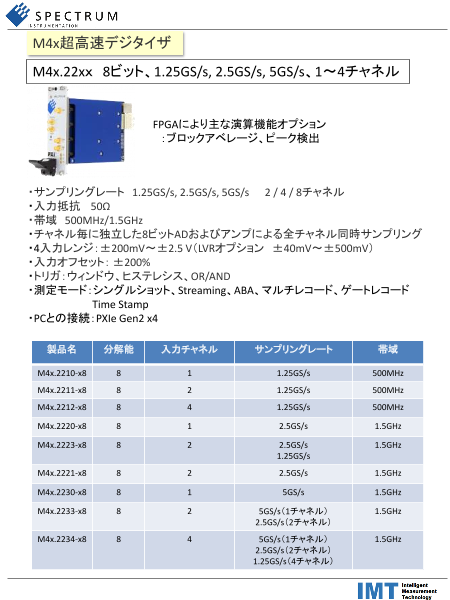
M4x超高速デジタイザ
M4x.22xx 8ビット、1.25GS/s, 2.5GS/s, 5GS/s、1~4チャネル
FPGAにより主な演算機能オプション
:ブロックアベレージ、ピーク検出
・サンプリングレート 1.25GS/s, 2.5GS/s, 5GS/s 2 / 4 / 8チャネル
・入力抵抗 50Ω
・帯域 500MHz/1.5GHz
・チャネル毎に独立した8ビットADおよびアンプによる全チャネル同時サンプリング
・4入力レンジ:±200mV~±2.5 V(LVRオプション ±40mV~±500mV)
・入力オフセット:±200%
・トリガ:ウィンドウ、ヒステレシス、OR/AND
・測定モード:シングルショット、Streaming、ABA、マルチレコード、ゲートレコード
Time Stamp
・PCとの接続:PXIe Gen2 x4
製品名 分解能 入力チャネル サンプリングレート 帯域
M4x.2210-x8 8 1 1.25GS/s 500MHz
M4x.2211-x8 8 2 1.25GS/s 500MHz
M4x.2212-x8 8 4 1.25GS/s 500MHz
M4x.2220-x8 8 1 2.5GS/s 1.5GHz
M4x.2223-x8 8 2 2.5GS/s 1.5GHz
1.25GS/s
M4x.2221-x8 8 2 2.5GS/s 1.5GHz
M4x.2230-x8 8 1 5GS/s 1.5GHz
M4x.2233-x8 8 2 5GS/s(1チャネル) 1.5GHz
2.5GS/s(2チャネル)
M4x.2234-x8 8 4 5GS/s(1チャネル) 1.5GHz
2.5GS/s(2チャネル)
1.25GS/s(4チャネル)
Page2
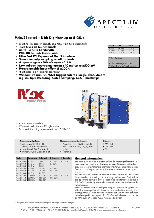
M4x.22xx-x4 - 8 bit Digitizer up to 5 GS/s
• 5 GS/s on one channel, 2.5 GS/s on two channels
• 1.25 GS/s on four channels Speed SNR ENOB5 GS/s >44.5 dB >7.1 bit
• up to 1.5 GHz bandwidth 2.5 GS/s >45.6 dB >7.3 bit
• PXIe 3U format, 2 slots wide 1.25 GS/ >46.9 dB >7.5 bit
• Ultra Fast PCI Express x4 Gen 2 interface
• Simultaneously sampling on all channels FPGA Options:
• 4 input ranges: ±200 mV up to ±2.5 V • Block Average up to 128k
• Low voltage input range option ±40 mV up to ±500 mV • Block Statistics/Peak Detect
• Programmable input offset of ±200%
• 4 GSample on-board memory
• Window, re-arm, OR/AND triggerFeatures: Single-Shot, Stream-
ing, Multiple Recording, Gated Sampling, ABA, Timestamps
• PXIe x4 Gen 2 Interface
• Works with all PXIe and PXI hybrid slots
• Sustained streaming mode more than 1.7 GB/s**
Operating Systems Recommended Software Drivers
• Windows 7 (SP1), 8, 10, • Visual C++, C++ Builder, Delphi • MATLAB
Server 2008 R2 and newer GNU C++, VB.NET, C#, J#, Java, • LabVIEW
• Linux Kernel 2.6, 3.x, 4.x, 5.x Python • IVI
• Windows/Linux 32 and 64 bit • SBench 6
Model Bandwidth 1 channel 2 channels 4 channels General Information
M4x.2234-x4 1.5 GHz 5 GS/s 2.5 GS/s 1.25 GS/s The M4x.22xx-x4 series digitizers deliver the highest performance in
M4x.2233-x4 1.5 GHz 5 GS/s 2.5 GS/s both speed and resolution. The series includes PXIe cards with either
M4x.2230-x4 1.5 GHz 5 GS/s one, two or four synchronous channels. The ADCs can sample at rates
M4x.2221-x4 1.5 GHz 2.5 GS/s 2.5 GS/s from 1.25 GS/s up to 5 GS/s with a maximum bandwidth of up to
M4x.2223-x4 1.5 GHz 2.5 GS/s 1.25 GS/s
M4x.2220-x4 1.5 GHz 2.5 GS/s 1.5 GHz.
M4x.2212-x4 500 MHz 1.25 GS/s 1.25 GS/s 1.25 GS/s The PXIe digitizers feature an interface with PCI Express x4 Gen 2 inter-
M4x.2211-x4 500 MHz 1.25 GS/s 1.25 GS/s face that offers outstanding data streaming performance. The interface
M4x.2210-x4 500 MHz 1.25 GS/s and Spectrums optimized drivers enable data transfer rates in excess of
1.7 GB/s** so that signals can be acquired, stored and analyzed at the
fastest speeds.
While the cards have been designed using the latest technology they are
still software compatible with the drivers from earlier Spectrum digitizers
starting with M2i series. Existing customers can use the same software
they developed for a 10 year old 200 kS/s multi-channel card and for
an M4x.22xx-x4 series 5 GS/s high speed digitizer!
**Throughput measured with a motherboard chipset supporting a TLP size of 256 bytes.SPECTRUM INSTRUMENTATION GMBH · AHRENSFELDER WEG 13-17 · 22927 GROSSHANSDORF · GERMANY 7.5.2020
PHONE: +49 (0)4102-6956-0 · FAX: +49 (0)4102-6956-66 · E-MAIL: info@spec.de · INTERNET: www.spectrum-instrumentation.com
Page3
Connections
• The cards are equipped with SMA connectors for the
Software Support analog signals as well as for the two external trigger
inputs, and clock input and output. In addition, there
Windows drivers are three MMCX connectors that are used for the
The cards are delivered with drivers for Windows 7, Windows 8 three multi-function I/O connectors. These multi-func-
and Windows 10 (32 bit and 64 bit). Programming examples for tion connectors can be individually programmed to
Visual C++, C++ Builder, Delphi, Visual Basic, VB.NET, C#, J#, Py- perform different functions:
thon, Java and IVI are included. • Trigger output
• Status output (armed, triggered, ready, ...)
Linux Drivers • Synchronous digital inputs, being stored inside the analog data
All cards are delivered with full Linux support. Pre com- samples
piled kernel modules are included for the most common • Asynchronous I/O lines
distributions like Fedora, Suse, Ubuntu LTS or Debian. The
Linux support includes SMP systems, 32 bit and 64 bit Input Amplifier
systems, versatile programming examples for GNU C++, The analog inputs can be adapt-
Python as well as the possibility to get the driver sources for your ed to real world signals using a
own compilation. wide variety of settings that are
individual for each channel. By
SBench 6 using software commands one
can select a matching input
A base license of SBench 6, the range and the signal offset can be compensated by programmable
easy-to-use graphical operating AC coupling or offset shifting.
software for Spectrum cards, is in-
cluded in the delivery. The base li-
cense makes it is possible to test Software selectable lowpass filter
the card, display acquired data Each analog channel contains a software selectable low-pass filter
and make some basic measure- to limit the input bandwidth. Reducing the analog input bandwidth
ments. It's a valuable tool for results in a lower total noise and can be useful especially with low
checking the card’s performance voltage input signals.
and assisting with the unit’s initial
setup. The cards also come with a demo license for the SBench 6 Automatic on-board calibration
professional version. This license gives the user the opportunity to Every channel of each card is calibrated in the factory before the
test the additional features of the professional version with their board is shipped. However, to compensate for environmental vari-
hardware. The professional version contains several advanced ations like PC power supply, temperature and aging the software
measurement functions, such as FFTs and X/Y display, import and driver includes routines for automatic offset and gain calibration.
export utilities as well as support for all acquisition modes including This calibration is performed on all input ranges of the "Buffered"
data streaming. Data streaming allows the cards to continuously ac- path and uses a high precision onboard calibration reference.
quire data and transfer it directly to the PC RAM or hard disk.
SBench 6 has been optimized to handle data files of several Digital inputs
GBytes. SBench 6 runs under Windows as well as Linux (KDE,
GNOME and Unity) operating systems. A test version of SBench 6 This option acquires additional syn-
can be downloaded directly over the internet and can run the pro- chronous digital channels phase-
fessional version in a simulation mode without any hardware in- stable with the analog data. As de-
stalled. Existing customers can also request a demo license for the fault a maximum of 3 additional
professional version from Spectrum. More details on SBench 6 can digital inputs are available on the front plate of the card using the
be found in the SBench 6 data sheet. multi-purpose I/O lines. An additional option offers 16 more digital
channels.
Third-party products Ring buffer mode
Spectrum supports the most popular third-party software products The ring buffer mode is the
such as LabVIEW, MATLAB or LabWindows/CVI. All drivers come standard mode of all oscillo-
with detailed documentation and working examples are included in scope instruments. Digitized
the delivery. Support for other software packages, like VEE or Da- data is continuously written
syLab, can also be provided on request. into a ring memory until a
trigger event is detected. After the trigger, post-trigger samples are
Hardware features and options recorded and pre-trigger samples can also be stored. The number
of pre-trigger samples available simply equals the total ring mem-
PXI Express x4 ory size minus the number of post trigger samples.
The M4x series PXI Express cards use a PCI Express
x4 Gen 2 connection. They can be used in every PXI FIFO mode
Express (PXIe) slot, as well as in any PXI hybrid slot The FIFO or streaming mode is designed for continuous data trans-
with Gen 1, Gen 2 or Gen 3. The maximum sustained fer between the digitizer card and the PC memory. When mounted
data transfer rate is more than 1.7 GByte/s (read di- in a PXI Express x4 Gen 2 capable PXIe slot, read streaming speeds
rection) or 1.4 GByte/s (write direction) per slot. of up to 1.7 GByte/s are possible. The control of the data stream is
done automatically by the driver on interrupt request basis. The
complete installed onboard memory is used to buffer the data, mak-
ing the continuous streaming process extremely reliable.
Page4
Channel trigger Firmware Option Block Average
The digitizers offer a wide variety of trigger modes. These include The Block Average Module im-
a standard triggering mode based on a signals level and slope, like proves the fidelity of noisy re-
that found in most oscilloscopes. It is also possible to define a win- petitive signals. Multiple
dow mode, with two trigger levels, that enables triggering when repetitive acquisitions with
signals enter or exit the window. Each input has its own trigger cir- very small dead-time are accu-
cuit which can be used to setup conditional triggers based on logi- mulated and averaged. Ran-
cal AND/OR patterns. All trigger modes can be combined with a dom noise is reduced by the
re-arming mode for accurate trigger recognition even on noisy sig- averaging process improving
nals. the visibility of the repetitive signal. The complete averaging pro-
cess is done inside the FPGA of the digitizer generating no CPU
External trigger input load at all. The amount of data is greatly decreased as well as the
All boards can be triggered using up to two external analog or dig- needed transfer bandwidth is heavily reduced.
ital signals. One external trigger input has two analog comparators
that can define an edge or window trigger, a hysteresis trigger or Please see separate data sheet for details on the firmware option.
a rearm trigger. The other input has one comparator that can be
used for standard edge and level triggers. Firmware Option Block Statistics (Peak Detect)
The Block Statistics and Peak
Multiple Recording Detect Module implements a
The Multiple Recording widely used data analysis and
mode allows the recording of reduction technology in hard-
several trigger events with an ware. Each block is scanned
extremely short re-arming for minimum and maximum
time. The hardware doesn’t peak and a summary includ-
need to be restarted in be- ing minimum, maximum, aver-
tween. The on-board memory is divided in several segments of the age, timestamps and position information is stored in memory. The
same size. Each of them is filled with data if a trigger event occurs. complete averaging process is done inside the FPGA of the digitiz-
Pre- and posttrigger of the segments can be programmed. The num- er generating no CPU load at all. The amount of data is greatly de-
ber of acquired segments is only limited by the used memory and creased as well as the needed transfer bandwidth is heavily
is unlimited when using FIFO mode. reduced.
Please see separate data sheet for details on the firmware option.
Gated Sampling
The Gated Sampling mode External clock input and output
allows data recording con-
trolled by an external gate Using a dedicated connector a sampling clock can be fed in from
signal. Data is only record- an external system. Additionally it’s also possible to output the in-
ed if the gate signal has a ternally used sampling clock on a separate connector to synchro-
programmed level. In addi- nize external equipment to this clock.
tion a pre-area before start
of the gate signal as well as a post area after end of the gate signal Reference clock
can be acquired. The number of gate segments is only limited by The option to use a precise
the used memory and is unlimited when using FIFO mode. external reference clock
(normally 10 MHz) is nec-
ABA mode essary to synchronize the
The ABA mode com- instrument for high-quality
bines slow continuous measurements with external equipment (like a signal source). It’s
data recording with fast also possible to enhance the quality of the sampling clock in this
acquisition on trigger way. The driver automatically generates the requested sampling
events. The ABA mode clock from the fed in reference clock.
works like a slow data
logger combined with a PXIe bus
fast digitizer. The exact The PXI Express bus (PCI Express eXtension for instrumentation) of-
position of the trigger events is stored as timestamps in an extra fers a variety of additional normed possibilities for synchronising
memory. different components in one system. It is posible to connect several
Spectrum cards with each other as well as to connect a Spectrum
Timestamp card with cards of other manufacturers.
The timestamp function
writes the time positions of PXI reference clock
the trigger events in an extra The card is able to use the 100 MHz low-jitter reference clock that
memory. The timestamps are is supplied by the PXIe system. Enabled by software the PXIe refer-
relative to the start of record- ence clock is fed into the on-board PLL. This feature allows the cards
ing, a defined zero time, ex- to run with a fixed phase relation.
ternally synchronized to a radio clock, an IRIG-B a GPS receiver.
Using the external synchronization gives a precise time relation for PXI trigger
acquisitions of systems on different locations. The Spectrum cards support star trigger as well as the PXI trigger
bus. Using a simple software commend one or more trigger lines
can be used as trigger source. This feature allows the easy setup of
OR connected triggers from different cards.
Page5
External Amplifiers
For the acquisition of extreme-
ly small voltage levels with a
high bandwidth a series of ex-
ternal amplifiers is available.
Each of the one channel am-
plifiers is working with a fixed
input impedance and allows -
depending on the bandwidth
- to select different amplifica-
tion levels between x10 (20
dB) up to x1000 (60 dB). Us-
ing the external amplifiers of the SPA series voltage levels in the uV
and mV area can be acquired.
Page6
Technical Data
Analog Inputs
Resolution 8 Bit
Input Type Single-ended
ADC Differential non linearity (DNL) ADC only ±0.35 LSB
ADC Integral non linearity (INL) ADC only ±0.9 LSB
ADC Bit Error Rate (BER) sampling rate 1.25 GS/s 10–16
Channel selection software programmable 1, 2, or 4 (maximum is model dependent)
Analog Input impedance fixed 50 Ω
Input Ranges (standard ranges) software programmable ±200 mV, ±500 mV, ±1 V, ±2.5 V (programmable input offset at 0%)
Input Ranges (Low Voltage Option) software programmable ±40 mV, ±100 mV, ±200 mV, ±500 mV (programmable input offset at 0%)
Programmable Input Offset software programmable ±200% of input range (allowing bi-polar ranges to become uni-polar)
Input Coupling software programmable AC/DC
Max DC voltage if AC coupling active ±30 V
Offset error (full speed) after warm-up and calibration < 0.5 LSB
Gain error (full speed) after warm-up and calibration < 2.0 LSB
Crosstalk 20 MHz sine signal (standard ranges) ≥ ±500 mV standard range < -96 dB (all channel same input range)
Crosstalk 20 MHz sine signal (standard ranges) = ±200 mV standard range < -88 dB (all channel same input range)
Crosstalk 100 MHz sine signal (standard ranges) ≥ ±500 mV standard range < -78 dB (all channel same input range)
Crosstalk 100 MHz sine signal (standard ranges) = ±200 mV standard range < -65 dB (all channel same input range)
Over voltage protection (standard ranges) input range ±200 mV ±500 mV ±1 V ±2.5 V
max. continuous input power 22.5 dBm 27.0 dBm 27.0 dBm 27.0 dBm
max. peak input voltage ±3 V ±7.5 V ±15 V ±30 V
Over voltage protection (low voltage option) input range ±40 mV ±100 mV ±200 mV ±500 mV
max. continuous input power 21.0 dBm 27.0 dBm 22.5 dBm 27.0 dBm
max. peak input voltage ±2.5 V ±6.25 V ±3 V ±7.5 V
Trigger
Available trigger modes software programmable Channel Trigger, External, Software, Window, Re-Arm, Or/And, Delay, PXI (M4x only)
Channel trigger level resolution software programmable 8 bit
Trigger engines 1 engine per channel with two individual levels, 2 external triggers
Trigger edge software programmable Rising edge, falling edge or both edges
Trigger delay software programmable 0 to (8GSamples - 32) = 8589934560 Samples in steps of 32 samples
Multi, ABA, Gate: re-arming time 1.25 GS/s or below 80 samples (+ programmed pretrigger)
2.5 GS/s 160 samples (+ programmed pretrigger)
5 GS/s 320 samples (+ programmed pretrigger)
Pretrigger at Multi, ABA, Gate, FIFO software programmable 32 up to 8192 Samples in steps of 32
Posttrigger software programmable 32 up to 16G samples in steps of 32 (defining pretrigger in standard scope mode)
Memory depth software programmable 64 up to [installed memory / number of active channels] samples in steps of 32
Multiple Recording/ABA segment size software programmable 64 up to [installed memory / 2 / active channels] samples in steps of 32
Trigger accuracy (all sources) 1 sample
Timestamp modes software programmable Standard, Startreset, external reference clock on X0 (e.g. PPS from GPS, IRIG-B)
Data format Std., Startreset: 64 bit counter, increments with sample clock (reset manually or on start)
RefClock: 24 bit upper counter (increment with RefClock)
40 bit lower counter (increments with sample clock, reset with RefClock)
Extra data software programmable none, acquisition of X0/X1/X2 inputs at trigger time, trigger source (for OR trigger)
Size per stamp 128 bit = 16 bytes
External trigger Ext0 Ext1
External trigger impedance software programmable 50 Ω /1 kΩ 1 kΩ
External trigger coupling software programmable AC or DC fixed DC
External trigger type Window comparator Single level comparator
External input level ±10 V (1 kΩ), ±2.5 V (50 Ω), ±10 V
External trigger sensitivity 2.5% of full scale range 2.5% of full scale range = 0.5 V
(minimum required signal swing)
External trigger level software programmable ±10 V in steps of 1 mV ±10 V in steps of 1 mV
External trigger maximum voltage ±30V ±30 V
External trigger bandwidth DC 50 Ω DC to 200 MHz n.a.
1 kΩ DC to 150 MHz DC to 200 MHz
External trigger bandwidth AC 50 Ω 20 kHz to 200 MHz n.a.
Minimum external trigger pulse width ≥ 2 samples ≥ 2 samples
Page7
Clock
Clock Modes software programmable internal PLL, external reference clock, Star-Hub sync (M4i only), PXI Reference Clock (M4x only)
Internal clock accuracy ≤ ±20 ppm
Clock setup granularity divider: maximum sampling rate divided by: 1, 2, 4, 8, 16, ... up to 262144
External reference clock range software programmable ≥ 10 MHz and ≤ 1.25 GHz
External reference clock input impedance 50 Ω fixed
External reference clock input coupling AC coupling
External reference clock input edge Rising edge
External reference clock input type Single-ended, sine wave or square wave
External reference clock input swing 0.3 V peak-peak up to 3.0 V peak-peak
External reference clock input max DC voltage ±30 V (with max 3.0 V difference between low and high level)
External reference clock input duty cycle requirement 45% to 55%
Clock setup granularity when using reference clock divider: maximum sampling rate divided by: 1, 2, 4, 8, 16, ... up to 262144
Internal reference clock output type Single-ended, 3.3V LVPECL
Internal reference clock output frequency 2.5 GHz / 64 = 39.0625 MHz
Star-Hub synchronization clock modes software selectable Internal clock (standard clock mode only), External reference clock
ABA mode clock divider for slow clock software programmable 16 up to (128k - 16) in steps of 16
Channel to channel skew on one card < 60 ps (typical)
Skew between star-hub synchronized cards < 130 ps (typical, preliminary)
M4i.223x M4i.222x M4i.221x
DN2.223-xx DN2.222-xx DN2.221-xx
DN2.225-xx DN6.221-xx
DN6.225-xx
ADC Resolution 8 bit 8 bit 8 bit
max sampling clock 5 GS/s 2.5 GS/s 1.25 GS/s
min sampling clock 4.768 kS/s 4.768 kS/s 4.768 kS/s
lower bandwidth limit (DC coupling) 0 Hz 0 Hz 0 Hz
lower bandwidth limit (AC coupling) < 30 kHz < 30 kHz < 30 kHz
-3 dB bandwidth (no filter active), Standard input ranges 1.5 GHz 1.5 GHz 500 MHz-
-3 dB bandwidth (no filter active), small input ranges, ir40m option installed 1.2 GHz 1.2 GHz 500 MHz-
-3 dB bandwidth (BW filter active) ~400 MHz ~400 MHz ~370 MHz
Block Average Signal Processing Option M4i.22xx/DN2.22x/DN6.22x Series
Firmware ≥ V1.14 (since August 2015) Firmware < V1.14
Data Mode (resulting sample width) software programmable 32 bit mode 16 bit mode 32 bit mode only
Minimum Waveform Length 64 samples 128 samples 64 samples
Minimum Waveform Stepsize 32 samples 64 samples 32 samples
Maximum Waveform Length 1 channel active 64 kSamples 128 kSamples 32 kSamples
Maximum Waveform Length 2 channels active 32 kSamples 64 kSamples 16 kSamples
Maximum Waveform Length 4 or more channels active 16 kSamples 32 kSamples 8 kSamples
Minimum Number of Averages 2 2 4
Maximum Number of Averages 16777216 (16M) 256 16777216 (16M)
Data Output Format fixed 32 bit signed integer 16 bit signed integer 32 bit signed integer
Re-Arming Time between waveforms 1.25 GS/s or below 80 samples (+ programmed pretrigger) 80 samples (+ programmed pretrigger)
Re-Arming Time between waveforms 2.5 GS/s 160 samples (+ programmed pretrigger) 160 samples (+ programmed pretrigger)
Re-Arming Time between waveforms 5 GS/s 320 samples (+ programmed pretrigger) 320 samples (+ programmed pretrigger)
Re-Arming Time between end of average to start of Depending on programmed segment length, 80/160/320 samples as above listed
next average max 50 µs
Block Statistics Signal Processing Option M4i.22xx/DN2.22x Series/DN6.22x Series
Minimum Waveform Length 64 samples
Minimum Waveform Stepsize 32 samples
Maximum Waveform Length Standard Acquisition 2 GSamples / channels
Maximum Waveform Length FIFO Acquisition 2 GSamples
Data Output Format fixed 32 bytes statistics summary
Statistics Information Set per Waveform Average, Minimum, Maximum, Position Minimum, Position Maximum, Trigger Timestamp
Re-Arming Time between Segments 1.25 GS/s or below 80 samples (+ programmed pretrigger)
Re-Arming Time between Segments 2.5 GS/s 160 samples (+ programmed pretrigger)
Re-Arming Time between Segments 5 GS/s 320 samples (+ programmed pretrigger)
Page8
Multi Purpose I/O lines (front-plate)
Number of multi purpose lines three, named X0, X1, X2
Input: available signal types software programmable Asynchronous Digital-In, Synchronous Digital-In, Timestamp Reference Clock
Input: impedance 10 kΩ to 3.3 V
Input: maximum voltage level -0.5 V to +4.0 V
Input: signal levels 3.3 V LVTTL
Input: bandwith 125 MHz
Output: available signal types software programmable Asynchronous Digital-Out, Trigger Output, Run, Arm, PLL Refclock, System Clock
Output: impedance 50 Ω
Output: signal levels 3.3 V LVTTL
Output: type 3.3V LVTTL, TTL compatible for high impedance loads
Output: drive strength Capable of driving 50 Ω loads, maximum drive strength ±48 mA
Output: update rate 14bit, 16 bit ADC resolution sampling clock
Output: update rate 8 bit ADC resolution Current sampling clock < 1.25 GS/s : sampling clock
Current sampling clock > 1.25 GS/s and < 2.50 GS/s : ½ sampling clock
Current sampling clock > 2.50 GS/s and < 5.00 GS/s : ¼ sampling clock
Dynamic Parameters
M4i.223x, M4x.223x and DN2.223-xx, DN2.225-xx and DN6.225-xx, 8 Bit 5 GS/s
Input Path DC or AC coupled, fixed 50 Ohm
Test signal frequency 10 MHz 40 MHz 70 MHz 240 MHz 600 MHz
Input Range ±200 mV ±500 mV ±1 V ±2.5 V ±200 mV ±1V ±200 mV ±1V ±200 mV ±1V ±200 mV ±1V
THD (typ) (dB <-60.2 dB <-60.3 dB -<60.3 dB <-60.3 dB <-58.9 dB <-58.2 dB <-58.8 dB <-58.0 dB <-54.0 dB <-54.0 dB <-45.0 dB <-46.3 dB
SNR (typ) (dB) >44.5 dB >44.8 dB >44.8 dB >44.5 dB >44.7 dB >44.7 dB >44.3 dB >44.3 dB >42.9 dB >42.9 dB >40.3 dB >40.2 dB
SFDR (typ), excl. harm. (dB) >53.7 dB >54.9 dB >54-9 dB >54.2 dB >50.3 dB >50.8 dB >50.2 dB >49.7 dB >49.4 dB >49.5 dB >44.3 dB >44.6 dB
SFDR (typ), incl. harm. (dB) >53.7 dB >54.7 dB >54.8 dB >54.2 dB >50.3 dB >50.8 dB >50.2 dB >49.7 dB >49.4 dB >49.5 dB >44.3 dB >44.6 dB
SINAD/THD+N (typ) (dB) >44.4 dB >44.7 dB >44.7 dB >44.4 dB >44.5 dB >44.4 dB >44.2 dB >44.1 dB >42.6 dB >42.6 dB >39.1 dB >39.3 dB
ENOB based on SINAD (bit) >7.1 bit >7.1 bit >7.1 bit >7.1 bit >7.1 bit >7.1 bit >7.1 bit >7.0 bit >6.8 bit >6.8 bit >6.2 bit >6.2 bit
ENOB based on SNR (bit) >7.1 bit >7.1 bit >7.1 bit >7.1 bit >7.1 bit >7.1 bit >7.1 bit >7.1 bit >6.9 bit >6.9 bit >6.4 bit >6.4 bit
M4i.222x, M4x.222x and DN2.222-xx, 8 Bit 2.5 GS/s
Input Path DC or AC coupled, fixed 50 Ohm
Test signal frequency 10 MHz 40 MHz 70 MHz 240 MHz 600 MHz
Input Range ±200 mV ±500 mV ±1 V ±2.5 V ±200 mV ±1V ±200 mV ±1V ±200 mV ±1V ±200 mV ±1V
THD (typ) (dB >-56.2 dB <-56.3 dB <-56.5 dB <-56.4 dB <-55.9 dB <-55.9 dB <-54.9 dB <-55.3 dB <-53.9 dB <-53.4 dB <-43.9 dB <-45.2 dB
SNR (typ) (dB) >45.6 dB >45.8 dB >45.6 dB >45.5 dB >44.7 dB >44.9 dB >44.5 dB >44.6 dB >43.9 dB >44.0 dB >42.1 dB >41.9 dB
SFDR (typ), excl. harm. (dB) >57.2 dB >57.3 dB >55.7 dB >55.1 dB >50.9 dB >50.5 dB >50.9 dB >50.6 dB >49.8 dB >49.0 dB >46.3 dB >45.2 dB
SFDR (typ), incl. harm. (dB) >56.5 dB >56.3 dB >55.1 dB >54.5 dB >50.9 dB >50.5 dB >50.9 dB >50.6 dB >49.8 dB >49.0 dB >45.2 dB >45.2 dB
SINAD/THD+N (typ) (dB) >45.2 dB >45.4 dB >45.3 dB >45.2 dB >44.4 dB >44.4 dB >44.2 dB >44.3 dB >43.5 dB >43.5 dB >39.9 dB >40.2 dB
ENOB based on SINAD (bit) >7.2 bit >7.3 bit >7.2 bit >7.2 bit >7.1 bit >7.1 bit >7.1 bit >7.1 bit >6.9 bit >6.9 bit >6.3 bit >6.4 bit
ENOB based on SNR (bit) >7.3 bit >7.3 bit >7.3 bit >7.3 bit >7.1 bit >7.1 bit >7.1 bit >7.1 bit >7.0 bit >7.0 bit >6.7 bit >6.7 bit
M4i.221x, M4x.221x, DN2.221 and DN6.221-xx, 8 Bit 1.25 GS/s - standard input ranges
Input Path DC or AC coupled, fixed 50 Ohm
Test signal frequency 10 MHz 40 MHz 70 MHz 240 MHz
Input Range ±200 mV ±500 mV ±1 V ±2.5 V ±200 mV ±1V ±200 mV ±1V ±200 mV ±1V
THD (typ) (dB <-59.0 dB <.58.9 dB <58.9 dB <59.0 dB <-53.6 dB <53.2 dB <-54.4 dB <-54.6 dB <-52.1 dB <-52.4 dB
SNR (typ) (dB) >46.9 dB >47.0 dB >47.0 dB >47.0 dB >46.8 dB >47.0 dB >47.0 dB >47.0 dB >46.1 dB >46.2 dB
SFDR (typ), excl. harm. (dB) >62.1 dB >62.1 dB >62.2 dB >62.0 dB >58.2 dB >59.8 dB >62.2 dB >61.9 dB >59.5 dB >58.5 dB
SFDR (typ), incl. harm. (dB) >60.7 dB >60.4 dB >60.5 dB >60.4 dB > 56.1 dB >56.2 dB > 57.7 dB >57.6 dB >52.5 dB >52.7 dB
SINAD/THD+N (typ) (dB) >46.6 dB >46.7 dB >46.7 dB >46.7 dB >46.0 dB >46.1 dB >46.3 dB >46.3 dB >45.1 dB >45.3 dB
ENOB based on SINAD (bit) >7.5 bit >7.5 bit >7.5 bit >7.5 bit >7.4 bit >7.4 bit >7.4 bit >7.4 bit >7.2 bit >7.2 bit
ENOB based on SNR (bit) >7.5 bit >7.5 bit >7.5 bit >7.5 bit >7.5 bit >7.5 bit >7.5 bit >7.5 bit >7.3 bit >7.4 bit
M4i.221x, M4x.221x and DN2.221-xx, 8 Bit 1.25 GS/s - low voltage input ranges
Input Path DC or AC coupled, fixed 50 Ohm
Test signal frequency 10 MHz 40 MHz 70 MHz 240 MHz
Input Range ±40 mV ±100 mV ±200 mV ±500 vV ±40 mV ±100 mV ±40 mV ±100 mV ±40 mV ±100 mV
THD (typ) (dB <-57.0 dB <.57.0 dB <.57.1 dB <.57.2 dB
SNR (typ) (dB) >44.0 dB >44.9 dB >44.9 dB >44.9 dB
SFDR (typ), excl. harm. (dB) >62.1 dB >62.1 dB >62.1 dB >62.2 dB
SFDR (typ), incl. harm. (dB) >60.1 dB >60.2 dB >60.2 dB >60.4 dB
SINAD/THD+N (typ) (dB) >44.0 dB >44.8 dB >44.8 dB >44.8 dB
ENOB based on SINAD (bit) >7.0 bit >7.2 bit >7.2 bit >7.2 bit
ENOB based on SNR (bit) >7.0 bit >7.2 bit >7.2 bit >7.2 bit
Dynamic parameters are measured at ±1 V input range (if no other range is stated) and 50Ω termination with the samplerate specified in the table. Measured parameters are averaged
20 times to get typical values. Test signal is a pure sine wave generated by a signal generator and a matching bandpass filter. Amplitude is >99% of FSR. SNR and RMS noise parameters
may differ depending on the quality of the used PC. SNR = Signal to Noise Ratio, THD = Total Harmonic Distortion, SFDR = Spurious Free Dynamic Range, SINAD = Signal Noise and Dis-
tortion, ENOB = Effective Number of Bits.
Page9
RMS Noise Level (Zero Noise)
M4i.223x, M4x.223x and DN2.223-xx, DN2.225-xx, DN6.225-xx, 8 Bit 5 GS/s
Input Range ±200 mV ±500 mV ±1 ±2.5 V
Voltage resolution (1 LSB) 1.6 mV 3.9 mV 7.8 mV 19.5 mV
DC, fixed 50 Ω, typical <0.3 LSB <0.5 mV <0.3 LSB <1.2 mV <0.3 LSB <2.3 mV <0.3 LSB <5.9 mV
DC, fixed 50 Ω, maximum <0.6 LSB <0.9 mV <0.6 LSB <2.3 mV <0.5 LSB <4.7 mV <0.5 LSB <11.7 mV
M4i.222x, M4x.222x and DN2.222-xx, 8 Bit 2.5 GS/s
Input Range ±200 mV ±500 mV ±1 ±2.5 V
Voltage resolution (1 LSB) 1.6 mV 3.9 mV 7.8 mV 19.5 mV
DC, fixed 50 Ω, typical <0.3 LSB <0.5 mV <0.3 LSB <1.2 mV <0.3 LSB <2.3 mV <0.3 LSB <5.9 mV
DC, fixed 50 Ω, maximum <0.6 LSB <0.9 mV <0.7 LSB <2.7 mV <0.5 LSB <4.7 mV <0.5 LSB <11.7 mV
Standard Version M4i.221x, M4x.221x and DN2.221-xx, 8 Bit 1.25 GS/s
Input Range ±200 mV ±500 mV ±1 ±2.5 V
Voltage resolution (1 LSB) 1.6 mV 3.9 mV 7.8 mV 19.5 mV
DC, fixed 50 Ω, typical <0.2 LSB <0.3 mV <0.2 LSB <0.8 mV <0.2 LSB <1.6 mV <0.2 LSB <3.9 mV
DC, fixed 50 Ω, maximum <0.3 LSB <0.5 mV <0.3 LSB <1.2 mV <0.3 LSB <2.3 mV <0.3 LSB <5.9 mV
Low Voltage Version M4i.221x, M4x.221x and DN2.221-xx, 8 Bit 1.25 GS/s
Input Range ±40 mV ±100 mV ±200 mV ±500 mV
Voltage resolution (1 LSB) 0.3 mV 0.8 mV 1.6 mV 3.9 mV
DC, fixed 50 Ω, typical <0.4 LSB <0.2 mV <0.4 LSB <0.3 mV <0.4 LSB <0.6 mV <0.4 LSB <1.6 mV
DC, fixed 50 Ω, maximum <0.5 LSB <0.2 mV <0.5 LSB <0.4 mV <0.5 LSB <0.8 mV <0.5 LSB <2.0 mV
Connectors
Analog Inputs/Analog Outputs SMA female (one for each single-ended input) Cable-Type: Cab-3mA-xx-xx
Trigger 0 Input SMA female Cable-Type: Cab-3mA-xx-xx
Clock Input SMA female Cable-Type: Cab-3mA-xx-xx
Trigger 1 Input SMA female Cable-Type: Cab-3mA-xx-xx
Clock Output SMA female Cable-Type: Cab-3mA-xx-xx
Multi Purpose I/O MMCX female (3 lines) Cable-Type: Cab-1m-xx-xx
Environmental and Physical Details
Dimension (Single Card) (PCB only) 160 mm x 100 mm (Standard 3U)
Width 2 slots
Weight (M4x.44xx series) maximum 340 g
Weight (M4x.22xx, M4x.66xx series) maximum 450 g
Warm up time 10 minutes
Operating temperature 0°C to 50°C
Storage temperature -10°C to 70°C
Humidity 10% to 90%
PXI Express specific details
PXIe slot type 4 Lanes, PCIe Gen 2 (x4 Gen2)
PXIe hybrid slot compatibility Fully compatible
Sustained streaming mode > 1.7 GB/s (measured with a chipset supporting a TLP size of 256 bytes, using PXIe x4 Gen2)
(Card-to-System: M4x.22xx, M4x.44xx)
Sustained streaming mode > 1.4 GB/s (measured with a chipset supporting a TLP size of 256 bytes, using PXIe x4 Gen2)
(System-to-Card: M4x.66xx)
Certification, Compliance, Warranty
EMC Immunity Compliant with CE Mark
EMC Emission Compliant with CE Mark
Product warranty 5 years starting with the day of delivery
Software and firmware updates Life-time, free of charge
Power Consumption
PCI EXPRESS
3.3V 12 V Total
M4x.2230-x4, M4x.2220-x4, M4x.2210-x4 0.25 A 2.6 A 32 W
M4x.2233-x4, M4x.2221-x4, 0.25 A 2.7 A 33 W
M4x.2223-x4, M4x.2211-x4
M4x.2234-x4, M4x.2212-x4 0.25 A 2.9 A 35 W
MTBF
MTBF 100000 hours
Page10
Hardware block diagram
Page11
Order Information
The card is delivered with 4 GSample on-board memory and supports standard acquisition (Scope), FIFO acquisition (streaming), Multiple
Recording, Gated Sampling, ABA mode and Timestamps. Operating system drivers for Windows/Linux 32 bit and 64 bit, examples for
C/C++, LabVIEW (Windows), MATLAB (Windows and Linux), IVI, .NET, Delphi, Java, Python and a Base license of the oscilloscope software
SBench 6 are included.
Adapter cables are not included. Please order separately!
PXI Express x4 Order no. Bandwidth Standard mem 1 channel 2 channels 4 channels
M4x.2210-x4 500 MHz 4 GSample 1.25 GS/s
M4x.2211-x4 500 MHz 4 GSample 1.25 GS/s 1.25 GS/s
M4x.2212-x4 500 MHz 4 GSample 1.25 GS/s 1.25 GS/s 1.25 GS/s
M4x.2220-x4 1.5 GHz 4 GSample 2.5 GS/s
M4x.2223-x4 1.5 GHz 4 GSample 2.5 GS/s 1.25 GS/s
M4x.2221-x4 1.5 GHz 4 GSample 2.5 GS/s 2.5 GS/s
M4x.2230-x4 1.5 GHz 4 GSample 5 GS/s
M4x.2233-x4 1.5 GHz 4 GSample 5 GS/s 2.5 GS/s
M4x.2234-x4 1.5 GHz 4 GSample 5 GS/s 2.5 GS/s 1.25 GS/s
Options Order no. Option
M4i.22xx-ir40m Low voltage input range option for 22xx series. 4 Input ranges with ±40 mV, ±100 mV, ±200 mV,
±500 mV, bandwidth limited.
Firmware Options Order no. Option
M4i.xxxx--spavg Signal Processing Firmware Option: Block Average (later firmware - upgrade available)
M4i.xxxx-spstat Signal Processing Firmware Option: Block Statistics/Peak Detect (later firmware - upgrade available)
Services Order no.
Recal Recalibration at Spectrum incl. calibration protocol
Standard Cables Order no.
for Connections Length to BNC male to BNC female to SMA male to SMA female to SMB female
Analog/Clock-In/Trig-In 80 cm Cab-3mA-9m-80 Cab-3mA-9f-80 Cab-3mA-3mA-80 Cab-3f-3mA-80
Analog/Clock-In/Trig-In 200 cm Cab-3mA-9m-200 Cab-3mA-9f-200 Cab-3mA-3mA-200 Cab-3f-3mA-200
Probes (short) 5 cm Cab-3mA-9f-5
Clk-Out/Trig-Out/Extra 80 cm Cab-1m-9m-80 Cab-1m-9f-80 Cab-1m-3mA-80 Cab-1m-3fA-80 Cab-1m-3f-80
Clk-Out/Trig-Out/Extra 200 cm Cab-1m-9m-200 Cab-1m-9f200 Cab-1m-3mA-200 Cab-1m-3fA-200 Cab-1m-3f-200
Information The standard adapter cables are based on RG174 cables and have a nominal attenuation of 0.3 dB/m at 100 MHz and
0.5 dB/m at 250 MHz. For high speed signals we recommend the low loss cables series CHF
Low Loss Cables Order No. Option
CHF-3mA-3mA-200 Low loss cables SMA male to SMA male 200 cm
CHF-3mA-9m-200 Low loss cables SMA male to BNC male 200 cm
Information The low loss adapter cables are based on MF141 cables and have an attenuation of 0.3 dB/m at 500 MHz and
0.5 dB/m at 1.5 GHz. They are recommended for signal frequencies of 200 MHz and above.
Amplifiers Order no. Bandwidth Connection Input Impedance Coupling Amplification
SPA.1841 (2) 2 GHz SMA 50 Ohm AC x100 (40 dB)
SPA.1801 (2) 2 GHz SMA 50 Ohm AC x10 (20 dB)
SPA.1601 (2) 500 MHz BNC 50 Ohm DC x10 (20 dB)
Information External Amplifiers with one channel, BNC/SMA female connections on input and output, manually adjustable offset, man-
ually switchable settings. An external power supply for 100 to 240 VAC is included. Please be sure to order an adapter
cable matching the amplifier connector type and matching the connector type for your A/D card input.
Software SBench6 Order no.
SBench6 Base version included in delivery. Supports standard mode for one card.
SBench6-Pro Professional version for one card: FIFO mode, export/import, calculation functions
SBench6-Multi Option multiple cards: Needs SBench6-Pro. Handles multiple synchronized cards in one system.
Volume Licenses Please ask Spectrum for details.
Software Options Order no.
SPc-RServer Remote Server Software Package - LAN remote access for M2i/M3i/M4i/M4x/M2p cards
SPc-SCAPP Spectrum’s CUDA Access for Parallel Processing - SDK for direct data transfer between Spectrum card
and CUDA GPU. Includes RDMA activation and examples. Signed NDA needed for access.
(1) : Just one of the options can be installed on a card at a time.
(2) : Third party product with warranty differing from our export conditions. No volume rebate possible.
Technical changes and printing errors possible
SBench, digitizerNETBOX and generatorNETBOX are registered trademarks of Spectrum Instrumentation GmbH. Microsoft, Visual C++, Windows, Windows 98, Windows NT, Window 2000, Windows XP, Windows Vista,
Windows 7, Windows 8 and Windows 10 are trademarks/registered trademarks of Microsoft Corporation. LabVIEW, DASYLab, Diadem and LabWindows/CVI are trademarks/registered trademarks of National Instruments
Corporation. MATLAB is a trademark/registered trademark of The Mathworks, Inc. Delphi and C++Builder are trademarks/registered trademarks of Embarcadero Technologies, Inc. Keysight VEE, VEE Pro and VEE OneLab
are trademarks/registered trademarks of Keysight Technologies, Inc. FlexPro is a registered trademark of Weisang GmbH & Co. KG. PCIe, PCI Express and PCI-X and PCI-SIG are trademarks of PCI-SIG. LXI is a registered
trademark of the LXI Consortium. PICMG and CompactPCI are trademarks of the PCI Industrial Computation Manufacturers Group. Oracle and Java are registered trademarks of Oracle and/or its affiliates. Intel and Intel Core
i3, Core i5, Core i7, Core i9 and Xeon are trademarks and/or registered trademarks of Intel Corporation. AMD, Opteron, Sempron, Phenom, FX, Ryzen and EPYC are trademarks and/or registered trademarks of Advanced
Micro Devices. NVIDIA, CUDA, GeForce, Quadro and Tesla are trademarks/registered trademarks of NVIDIA Corporation.