


DI M4i.77xx 32チャネル、125MB/s, 250MB/s, 720MB/s
DI M4i.77xx 32チャネル、125MB/s, 250MB/s, 720MB/s
このカタログについて
| ドキュメント名 | DI M4i.77xx 32チャネル、125MB/s, 250MB/s, 720MB/s |
|---|---|
| ドキュメント種別 | 製品カタログ |
| ファイルサイズ | 1.1Mb |
| 登録カテゴリ | |
| 取り扱い企業 | 株式会社エレクトロニカ IMT事業部 (この企業の取り扱いカタログ一覧) |
この企業の関連カタログ


このカタログの内容
Page1
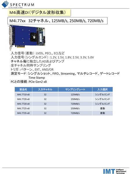
M4i高速DI(デジタル波形収集)
M4i.77xx 32チャネル、125MB/s, 250MB/s, 720MB/s
入力信号(差動):LVDS、PECL、ECLなど
入力信号(シングルエンド):1.2V, 1.5V, 1.8V, 2.5V, 3.3V, 5.0V
チャネル毎に独立したADおよびアンプ
全チャネル同時サンプリング
トリガ:パターン、EXT、AND/OR
測定モード:シングルショット、FIFO、Streaming、マルチレコード、ゲートレコード
Time Stamp
PCとの接続:PCIe Gen2 x8
製品名 入力チャネル サンプリングレート 入力選択
M4i.7710-x8 32 125MB/s シングルエンド
M4i.7720-x8 32 250MB/s シングルエンド
M4i.7720-x8 32 720MB/s シングルエンド
M4i.7725-x8 32 250MB/s 差動
M4i.7735-x8 32 720MB/s 差動
Page2
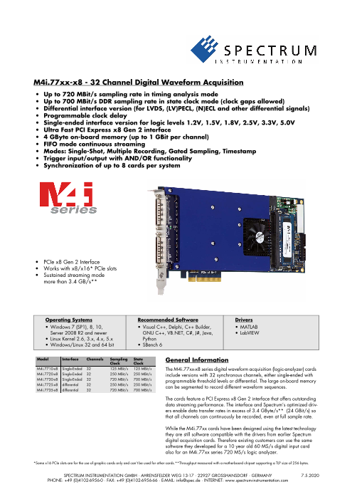
M4i.77xx-x8 - 32 Channel Digital Waveform Acquisition
• Up to 720 MBit/s sampling rate in timing analysis mode
• Up to 700 MBit/s DDR sampling rate in state clock mode (clock gaps allowed)
• Differential interface version (for LVDS, (LV)PECL, (N)ECL and other differential signals)
• Programmable clock delay
• Single-ended interface version for logic levels 1.2V, 1.5V, 1.8V, 2.5V, 3.3V, 5.0V
• Ultra Fast PCI Express x8 Gen 2 interface
• 4 GByte on-board memory (up to 1 GBit per channel)
• FIFO mode continuous streaming
• Modes: Single-Shot, Multiple Recording, Gated Sampling, Timestamp
• Trigger input/output with AND/OR functionality
• Synchronization of up to 8 cards per system
• PCIe x8 Gen 2 Interface
• Works with x8/x16* PCIe slots
• Sustained streaming mode
more than 3.4 GB/s**
Operating Systems Recommended Software Drivers
• Windows 7 (SP1), 8, 10, • Visual C++, Delphi, C++ Builder, • MATLAB
Server 2008 R2 and newer GNU C++, VB.NET, C#, J#, Java, • LabVIEW
• Linux Kernel 2.6, 3.x, 4.x, 5.x Python
• Windows/Linux 32 and 64 bit • SBench 6
Model Interface Channels Sampling State General Information
Clock Clock
M4i.7710-x8 Single-Ended 32 125 MBit/s 125 MBit/s The M4i.77xx-x8 series digital waveform acquisition (logic-analyzer) cards
M4i.7720-x8 Single-Ended 32 250 MBit/s 250 MBit/s include versions with 32 synchronous channels, either single-ended with
M4i.7730-x8 Single-Ended 32 720 MBit/s 700 MBit/s programmable threshold levels or differential. The large on-board memory
M4i.7725-x8 differential 32 250 MBit/s 250 MBit/s can be segmented to record different waveform sequences.
M4i.7735-x8 differential 32 720 MBit/s 700 MBit/s
The cards feature a PCI Express x8 Gen 2 interface that offers outstanding
data streaming performance. The interface and Spectrum’s optimized driv-
ers enable data transfer rates in excess of 3.4 GByte/s** (24 GBit/s) so
that all channels can continuously be recorded, even at full sample rate.
While the M4i.77xx cards have been designed using the latest technology
they are still software compatible with the drivers from earlier Spectrum
digital acquisition cards. Therefore existing customers can use the same
software they developed for a 10 year old 60 MS/s digital input card
also for an M4i.77xx series 720 MS/s logic analyzer.
*Some x16 PCIe slots are for the use of graphic cards only and can’t be used for other cards.**Throughput measured with a motherboard chipset supporting a TLP size of 256 bytes.SPECTRUM INSTRUMENTATION GMBH · AHRENSFELDER WEG 13-17 · 22927 GROSSHANSDORF · GERMANY 7.5.2020
PHONE: +49 (0)4102-6956-0 · FAX: +49 (0)4102-6956-66 · E-MAIL: info@spec.de · INTERNET: www.spectrum-instrumentation.com
Page3
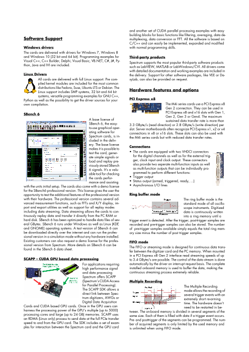
and another set of CUDA parallel processing examples with easy
building blocks for basic functions like filtering, averaging, data de-
Software Support multiplexing, data conversion or FFT. All the software is based on
C/C++ and can easily be implemented, expanded and modified
Windows drivers with normal programming skills.
The cards are delivered with drivers for Windows 7, Windows 8
and Windows 10 (32 bit and 64 bit). Programming examples for Third-party products
Visual C++, C++ Builder, Delphi, Visual Basic, VB.NET, C#, J#, Py- Spectrum supports the most popular third-party software products
thon, Java and IVI are included. such as LabVIEW, MATLAB or LabWindows/CVI. All drivers come
with detailed documentation and working examples are included in
Linux Drivers the delivery. Support for other software packages, like VEE or Da-
All cards are delivered with full Linux support. Pre com- syLab, can also be provided on request.
piled kernel modules are included for the most common
distributions like Fedora, Suse, Ubuntu LTS or Debian. The
Linux support includes SMP systems, 32 bit and 64 bit Hardware features and options
systems, versatile programming examples for GNU C++,
Python as well as the possibility to get the driver sources for your PCI Express x8
own compilation. The M4i series cards use a PCI Express x8
Gen 2 connection. They can be used in
SBench 6 PCI Express x8 and x16 slots with Gen 1,
Gen 2, Gen 3 or Gen4. The maximum
A base license of sustained data transfer rate is more than
SBench 6, the easy- 3.3 GByte/s (read direction) or 2.8 GByte/s (write direction) per
to-use graphical oper- slot. Server motherboards often recognize PCI Express x1, x2 or x4
ating software for connections in x8 or x16 slots. These slots can also be used with
Spectrum cards, is in- the M4i series cards but with reduced data transfer rates.
cluded in the deliv-
ery. The base license
makes it is possible to Connections
test the card, gener- • The cards are equipped with two VHDCI connectors
ate simple signals or for the digital channels as well as for the external trig-
load and replay pre- ger, clock input and clock output. These connectors
viously stored SBench also provide two seperate multi-function inputs as well
6 signals. It's a valu- as multi-function outputs that can be individually pro-
able tool for checking grammed to perform different functions:
the cards perfor- • Trigger output
mance and assisting • Status output (armed, triggered, ready, ...)
with the units initial setup. The cards also come with a demo license • Asynchronous I/O lines
for the SBench6 professional version. This license gives the user the
opportunity to test the additional features of the professional version Ring buffer mode
with their hardware. The professional version contains several ad- The ring buffer mode is the
vanced measurement functions, such as FFTs and X/Y display, im- standard mode of all oscillo-
port and export utilities as well as support for all replay modes scope instruments. Digitized
including data streaming. Data streaming allows the cards to con- data is continuously written
tinuously replay data and transfer it directly from the PC RAM or into a ring memory until a
hard disk. SBench 6 has been optimized to handle data files of sev- trigger event is detected. After the trigger, post-trigger samples are
eral GBytes. SBench 6 runs under Windows as well as Linux (KDE recorded and pre-trigger samples can also be stored. The number
and GNOME) operating systems. A test version of SBench 6 can of pre-trigger samples available simply equals the total ring mem-
be downloaded directly over the internet and can run the profes- ory size minus the number of post trigger samples.
sional version in a simulation mode without any hardware installed.
Existing customers can also request a demo license for the profes- FIFO mode
sional version from Spectrum. More details on SBench 6 can be
found in the SBench 6 data sheet. The FIFO or streaming mode is designed for continuous data trans-fer between the digitizer card and the PC memory. When mounted
in a PCI Express x8 Gen 2 interface read streaming speeds of up
SCAPP – CUDA GPU based data processing to 3.4 GByte/s are possible. The control of the data stream is done
For applications requiring automatically by the driver on interrupt request basis. The complete
high performance signal installed onboard memory is used to buffer the data, making the
and data processing continuous streaming process extremely reliable.
Spectrum offers SCAPP
(Spectrum’s CUDA Access Multiple Recording
for Parallel Processing). The Multiple Recording
The SCAPP SDK allows a mode allows the recording of
direct link between Spec- several trigger events with an
trum digitizers, AWGs or extremely short re-arming
Digital Data Acquisition time. The hardware doesn’t
Cards and CUDA based GPU cards. Once in the GPU users can need to be restarted in be-
harness the processing power of the GPU’s multiple (up to 5000) tween. The on-board memory is divided in several segments of the
processing cores and large (up to 24 GB) memories. SCAPP uses same size. Each of them is filled with data if a trigger event occurs.
an RDMA (Linux only) process to send data at the full PCIe transfer Pre- and posttrigger of the segments can be programmed. The num-
speed to and from the GPU card. The SDK includes a set of exam- ber of acquired segments is only limited by the used memory and
ples for interaction between the Spectrum card and the GPU card is unlimited when using FIFO mode.
Page4
Gated Sampling Star-Hub
The Gated Sampling mode The Star-Hub is an additional module
allows data recording con- allowing the phase stable synchroniza-
trolled by an external gate tion of up to 8 boards of a kind in one
signal. Data is only record- system. Independent of the number of
ed if the gate signal has a boards there is no phase delay be-
programmed level. In addi- tween all channels. The Star-Hub dis-
tion a pre-area before start tributes trigger and clock information
of the gate signal as well as a post area after end of the gate signal between all boards to ensure all con-
can be acquired. The number of gate segments is only limited by nected boards are running with the
the used memory and is unlimited when using FIFO mode. same clock and trigger. All trigger
sources can be combined with a logical OR allowing all channels
Timestamp of all cards to be the trigger source at the same time.
The timestamp function
writes the time positions of
the trigger events in an extra
memory. The timestamps are
relative to the start of record-
ing, a defined zero time, ex-
ternally synchronized to a radio clock, an IRIG-B a GPS receiver.
Using the external synchronization gives a precise time relation for
acquisitions of systems on different locations.
Pattern trigger
Pattern triggers can be defined for every bit of the digital input da-
ta. Each input for the pattern trigger can be set to high or low, de-
pending on the expected level, or "don't care". In addition, edge
detection can be used to allow triggering on rising , falling or both
edges. The pattern trigger can be used to recognize a huge variety
of trigger events.
External trigger input
The boards can be triggered using an external trigger input, that
has the same exact interface capabilities as the installed data lines,
either single-ended with programmable threshold or differential.
External clock input and output
Using a dedicated input line, that has the same exact interface ca-
pabilities as the installed data lines (either single-ended with pro-
grammable threshold or differential) a sampling clock can be fed in
from an external system. Additionally it’s also possible to output the
internally used sampling clock on a separate line to synchronize ex-
ternal equipment to this clock.
State clock
The state analysis mode allows to use an external clock to synchro-
nously sample the applied data. In this mode the clock is allowed
to have gaps, as long as the minimum required high and low times
are met. To simplify the synchronous sampling of the data, the in-
coming clock signal can be shifted/delayed with regards to the da-
ta, to allow proper data capture.
Reference clock
The option to use a precise
external reference clock
(typically 10 MHz) is nec-
essary to synchronize the
instrument for high-quality
measurements with external equipment (like a signal source). It’s
also possible to enhance the stability of the sampling clock in this
way. The driver automatically generates the requested sampling
clock from the fed in reference clock.
Page5
Technical Data
Differential Interface
Available inputs Data D0 to D31, Trigger (TrigIn), Strobe, Clock (ClkIn), X0, X1
Data Channel Selection software programmable 32 channels, 16 channels, 8 channels
Data/Control Input Compatibility LVDS, LVPECL, PECL, (N)ECL, universal differential inputs
Input Coupling DC
Input Type high-speed comparator
Input maximum voltage levels -3.0 V to +5.0 V, max difference between inputs ±8 V
Input voltage hysteresis 25 mV
Input termination differential termination with 125 Ω
Open inputs fail save -> defined and fixed input level with open inputs, no external termination necessary
Available outputs Clock (ClkOut), Trigger (TrigOut), X0, X1
Output signal type LVDS
Single-Ended Interface
Available inputs Data D0..D31, Trigger (TrigIn), Strobe, Clock (ClkIn), Multi-Purpose In (X0,X1) + Out (X0,X1,X2)
Data Channel Selection software programmable 32 channels, 16 channels, 8 channels
Data/Control Input Compatibility compatible to 1.2V, 1.5V, 1.8V, 2.5V, 3.3V, 5.0V (LV)TTL and (LV)CMOS logic levels
Input Coupling DC
Input Type high-speed comparator
Input threshold level software programmable 0.0 V up to 4.0 V in steps of 10 mV, separately programmable for
(D0..D7), (D8..D15), (D16..D23), (D24..D31), TrigIn, ClkIn, StrobeIn, (X0..X1)
Input maximum voltage levels -3.0 V to +5.0 V
Input voltage hysteresis 25 mV
Input termination software programmable 75 Ω (to GND) / 4.7 kΩ (to GND) separately programmable for
(D0..D7), (D8..D15), (D16..D23), (D24..D31), TrigIn, ClkIn, StrobeIn, X0, X1
Open inputs fail save -> defined and fixed input level with open inputs, no external termination necessary
Available outputs Clock (ClkOut), Multi-Purpose Out (X0, X1, X2)
Output signal type 3.3V LVTTL compatible
Trigger
Available trigger sources software programmable External trigger, pattern trigger, software
Trigger edge software programmable Rising edge, falling edge or both edges
Trigger delay software programmable 0 to (8GSamples - 32) = 8589934576 Samples in steps of 32 samples
Multi, Gate: re-arming time 40 samples (+ programmed pretrigger)
Pretrigger at Multi, Gate, FIFO software programmable 32 up to 4096 samples in steps of 32
Posttrigger software programmable 32 up to 8G samples in steps of 32 (defining pretrigger in standard scope mode)
Memory depth software programmable 32 up to [installed memory / number of active channels] samples in steps of 32
Multiple Recording segment size software programmable 32 up to [installed memory / 2 / active channels] samples in steps of 32
Internal/External trigger accuracy 1 sample
Timestamp modes software programmable Standard, Startreset, external reference clock on X1 (e.g. PPS from GPS, IRIG-B)
Data format Std., Startreset: 64 bit counter, increments with sample clock (reset manually or on start)
RefClock: 24 bit upper counter (increment with RefClock)
40 bit lower counter (increments with sample clock, reset with RefClock)
Extra data software programmable none, acquisition of X0/X1 inputs at trigger time
Size per stamp 128 bit = 16 bytes
Multi Purpose I/O lines (on VHDCI connector)
Number of multi purpose lines three named X0 and X1, separate lines for input and output, X2 (output only)
Input: available signal types software programmable Asynchronous Digital-In, Timestamp Reference Clock
Output: available signal types software programmable Asynchronous Digital-Out, Run, Arm, Trigger, PLL RefClk
Multi Purpose input impedance (Diff.) differential termination with 125 Ω
Multi Purpose input impedance (SE) software programmable 75 Ω (to GND) / 4.7 kΩ (to GND), separately programmable for X0 and X1
Multi Purpose input type (Diff.) LVDS, LVPECL, PECL, (N)ECL, universal differential inputs
Multi Purpose input type (SE) compatible to 1.2V, 1.5V, 1.8V, 2.5V, 3.3V, 5.0V (LV)TTL and (LV)CMOS logic levels
Multi Purpose input threshold level (SE) software programmable 0.0 V up to 4.0 V in steps of 10 mV (common programmable level for X0 and X1)
Multi Purpose output type (Diff.) Differential LVDS
Multi Purpose output type (SE) 3.3V LVTTL compatible
Power Source (on VHDCI connector)
Number of power pins 6
Voltage 3.3 V
Maximum current 500 mA combined on all pins
Fuse Self resetting fuse (PTC)
Page6
Clock
Clock Modes software programmable internal PLL, external reference clock, state clock, sync
Internal clock accuracy ≤ ±20 ppm
Internal clock setup granularity 1 Hz
Clock setup range gaps 562 MHz to 574 MHz (no clock setup possible in that range)
Primary Clk-In (Ext0) as reference clock
External reference clock range software programmable ≥ 10 MHz and ≤ 1 GHz
External reference clock input impedance (Diff.) differential termination with 125 Ω
External reference clock input type (Diff.) LVDS, LVPECL, PECL, (N)ECL, universal differential inputs
External reference clock input type (SE) compatible to 1.2V, 1.5V, 1.8V, 2.5V, 3.3V, 5.0V (LV)TTL and (LV)CMOS logic levels
External reference clock input impedance (SE) software programmable 75 Ω (to GND) / 4.7 kΩ (to GND)
External reference clock input threshold level (SE) software programmable 0.0 V up to 4.0 V in steps of 10 mV
External reference clock input edge Rising edge
External reference clock input duty cycle requirement 45% to 55%
External reference clock input requirements no frequency changes, no gaps
Primary Clk-In (Ext0) as state clock
External state clock input coupling DC
External state clock input impedance (Diff.) differential termination with 125 Ω
External state clock input impedance (SE) software programmable 75 Ω (to GND) / 4.7 kΩ (to GND)
External state clock input type (Diff.) LVDS, LVPECL, PECL, (N)ECL, universal differential inputs
External state clock input type (SE) compatible to 1.2V, 1.5V, 1.8V, 2.5V, 3.3V, 5.0V (LV)TTL and (LV)CMOS logic levels
External state clock input threshold level (SE) software programmable 0.0 V up to 4.0 V in steps of 10 mV
External state clock input edge software programmable Rising edge or falling edge (SDR) or both edges (DDR)
External state clock input requirements Any frequency within specification, changes allowed, gaps allowed, DC allowed
External state clock delay software programmable 0 ps to 2000 ps with a step size of 40 ps
Secondary Clk-In-AC (Ext1) as state clock
External secondary clock input coupling AC
External secondary clock input impedance differential termination with 100 Ω
External secondary clock input type LVPECL
External secondary clock input voltage swing (ClkIn-AC+ to ClkIn-AC–): ±100 mV up to ±1.7 V
Sampling clock output type (Diff.) Differential LVDS
Sampling clock output type (SE) 3.3V LVTTL compatible
Sampling clock output frequency Internal or External reference ½ of internal sampling clock (disabled for frequencies above 125 MHz on SE models)
Sampling clock output frequency External state clock Copy of fed in state clock (not available for M4i.7730)
Star-Hub synchronization clock modes software selectable Internal clock, External reference clock (state clock is not available with synchronization)
Clock Limits
M4i.7710-x8 M4i.7720-x8 M4i.7730-x8 M4i.7725-x8 M4i.7735-x8
Interface Single-Ended Single-Ended Single-Ended Differential Differential
minimum internal clock 610 S/s 610 S/s 610 S/s 610 S/s 610 S/s
maximum internal clock 125 MS/s 250 MS/s 720 MS/s 250 MS/s 720 MS/s
minimum state clock (Ext 0) DC DC DC DC DC
minimum state clock (Ext 1) 30 kHz 30 kHz 30 kHz 30 kHz 30 kHz
maximum state clock (single data rate) 125 MHz 250 MHz 350 MHz 250 MHz 350 MHz
maximum state clock (double data rate) 62.5 MHz 125 MHz 350 MHz 125 MHz 350 MHz
maximum state clock data rate (SDR) 125 MBit/s 250 MBit/s 350 MBit/s 250 MBit/s 350 MBit/s
maximum state clock data rate (DDR) 125 MBit/s 250 MBit/s 700 MBit/s 250 MBit/s 700 MBit/s
Timings
Signal type External reference clock Input State Clock Input State Clock Input
Ext 0 Ext 0 Ext 1
No Clk Delay No Clk Delay Max. Clk Delay No Clk Delay Max. Clk Delay
tsetup Setup time before clock edge input signals TBD 720 ps -1280 ps TBD TBD
thold Hold time after clock edge input signals TBD 200 ps 2200 ps TBD TBD
tdelay Delay from clock input to clock input signals TBD TBD TBD TBD TBD
output
Connectors
Number of connectors 2
Connector type 68 pin standard VHDCI
Connector impedance 125 Ω (differential), 75 Ω (single-ended),
Cable recommendations compatible to SCSI ultra-320, double shielded, twisted pair, max length 1 m,
cable drilling: Pin1/Pin35, Pin2/Pin36 ... Pin 34/68
Page7
Environmental and Physical Details
Dimension (Single Card) 241 mm (¾ PCIe length) x 107 mm x 20 mm (single slot width)
Dimension (Card with option SH8tm installed) 241 mm (¾ PCIe length) x 107 mm x 40 mm (double slot width)
Dimension (Card with option SH8ex installed) 312 mm (full PCIe length) x 107 mm x 20 mm (single slot width)
Weight (M4i.44xx series) maximum 290 g
Weight (M4i.22xx, M4i.66xx, M4i.77xx series) maximum 420 g
Weight (Option star-hub -sh8ex, -sh8tm) including 8 sync cables 130 g
Warm up time 10 minutes
Operating temperature 0°C to 50°C
Storage temperature -10°C to 70°C
Humidity 10% to 90%
PCI Express specific details
PCIe slot type x8 Generation 2
PCIe slot compatibility (physical) x8/x16
PCIe slot compatibility (electrical) x1, x2, x4, x8, x16 with Generation 1, Generation 2, Generation 3, Generation 4
Sustained streaming mode > 3.4 GB/s (measured with a chipset supporting a TLP size of 256 bytes, using PCIe x8 Gen2)
(Card-to-System: M4i.22xx, M4i.44xx, M4i.77xx)
Sustained streaming mode > 2.8 GB/s (measured with a chipset supporting a TLP size of 256 bytes, using PCIe x8 Gen2)
(System-to-Card: M4i.66xx)
Certification, Compliance, Warranty
EMC Immunity Compliant with CE Mark
EMC Emission Compliant with CE Mark
Product warranty 5 years starting with the day of delivery
Software and firmware updates Life-time, free of charge
Power Consumption
PCI EXPRESS
3.3V 12 V Total
M4i.771x-x8, M4i.772x-x8 Power output 0mA 0.2 A 2.9 A 36 W
M4i.773x-x8 Power output 0mA 0.2 A 3.1 A 38 W
MTBF
MTBF 100000 hours
Block diagram differential input version
Page8
Block diagram single-ended input version
Order Information
The card is delivered with 4 GByte on-board memory and supports standard acquisition (Scope), FIFO acquisition (streaming), Multiple Re-
cording, Gated Sampling and Timestamps. Operating system drivers for Windows/Linux 32 bit and 64 bit, examples for
C/C++, LabVIEW (Windows), MATLAB (Windows and Linux), .NET, Delphi, Java, Python and a Base license of the oscilloscope/logic-ana-
lyzer software SBench 6 are included.
Adapter cables are not included. Please order separately!
PCI Express x8 Order no. Channels Interface Standard mem Sampling Clock State Clock
M4i.7710-x8 32 Single-Ended 4 GByte 125 MBit/s 125 MBit/s
M4i.7720-x8 32 Single-Ended 4 GByte 250 MBit/s 250 MBit/s
M4i.7730-x8 32 Single-Ended 4 GByte 720 MBit/s 700 MBit/s
M4i.7725-x8 32 Differential 4 GByte 250 MBit/s 250 MBit/s
M4i.7735-x8 32 Differential 4 GByte 720 MBit/s 700 MBit/s
Options Order no. Option
M4i.xxxx-SH8ex (1) Synchronization Star-Hub for up to 8 cards (extension), only one slot width, extension of the card to
full PCI Express length (312 mm). 8 synchronization cables included.
M4i.xxxx-SH8tm (1) Synchronization Star-Hub for up to 8 cards (top mount), two slots width, top mounted on card. 8 syn-
chronization cables included.
M4i-upgrade Upgrade for M4i.xxxx: Later installation of option Star-Hub
VHDCI Cable Order no. Option
Cab-v68-v68-100 Shieleded twisted-pair cable VHDCI to VHDCI, 100 cm, 125 Ω differentiell, 90 Ω single-ended
Cab-v68-v68-300 Shieleded twisted-pair cable VHDCI to VHDCI, 300 cm, 125 Ω differentiell, 90 Ω single-ended
Software SBench6 Order no.
SBench6 Base version included in delivery. Supports standard mode for one card.
SBench6-Pro Professional version for one card: FIFO mode, export/import, calculation functions
SBench6-Multi Option multiple cards: Needs SBench6-Pro. Handles multiple synchronized cards in one system.
Volume Licenses Please ask Spectrum for details.
Software Options Order no.
SPc-RServer Remote Server Software Package - LAN remote access for M2i/M3i/M4i/M4x/M2p cards
SPc-SCAPP Spectrum’s CUDA Access for Parallel Processing - SDK for direct data transfer between Spectrum card
and CUDA GPU. Includes RDMA activation and examples. Signed NDA needed for access.
(1) : Just one of the options can be installed on a card at a time.
(2) : Third party product with warranty differing from our export conditions. No volume rebate possible.
Technical changes and printing errors possible
SBench, digitizerNETBOX and generatorNETBOX are registered trademarks of Spectrum Instrumentation GmbH. Microsoft, Visual C++, Windows, Windows 98, Windows NT, Window 2000, Windows XP, Windows Vista,
Windows 7, Windows 8 and Windows 10 are trademarks/registered trademarks of Microsoft Corporation. LabVIEW, DASYLab, Diadem and LabWindows/CVI are trademarks/registered trademarks of National Instruments
Corporation. MATLAB is a trademark/registered trademark of The Mathworks, Inc. Delphi and C++Builder are trademarks/registered trademarks of Embarcadero Technologies, Inc. Keysight VEE, VEE Pro and VEE OneLab
are trademarks/registered trademarks of Keysight Technologies, Inc. FlexPro is a registered trademark of Weisang GmbH & Co. KG. PCIe, PCI Express and PCI-X and PCI-SIG are trademarks of PCI-SIG. LXI is a registered
trademark of the LXI Consortium. PICMG and CompactPCI are trademarks of the PCI Industrial Computation Manufacturers Group. Oracle and Java are registered trademarks of Oracle and/or its affiliates. Intel and Intel Core
i3, Core i5, Core i7, Core i9 and Xeon are trademarks and/or registered trademarks of Intel Corporation. AMD, Opteron, Sempron, Phenom, FX, Ryzen and EPYC are trademarks and/or registered trademarks of Advanced
Micro Devices. NVIDIA, CUDA, GeForce, Quadro and Tesla are trademarks/registered trademarks of NVIDIA Corporation.