


幅広いモジュール入出力で最も効率的な高精度計測機能を備えたシグナル・チェーン・ソリューション
アナログ・デバイセズは、産業用高精度信号計測ソリューションのリーディング・サプライヤです。これらのソリューションは、化学および医薬品、炭化水素(石油およびガス)、環境(廃水および処理)、オートモーティブなど、幅広い産業の処理および製造プラント、機械の PLC、DCS システムのオートメーション・コントローラ・モジュールに組み込まれています。定評のある産業用アプリケーションのシステム知識と、高性能、低消費電力、高集積が特長の包括的な製品ポートフォリオを有するアナログ・デバイセズは、オートメーション・コントローラの設計エンジニアにとって重要なパートナーです。
【ラインナップ】
◆アナログ入力温度モジュール
◆アナログ入力絶縁モジュール
◆アナログ入力チャンネル間絶縁モジュール
◆アナログ出力絶縁モジュール
◆アナログ出力チャンネル間絶縁モジュール
◆詳細はカタログをダウンロードしご覧いただくか、お気軽にお問い合わせ下さい。
このカタログについて
| ドキュメント名 | オートメーション・コントローラ設計向け製品およびシグナル・チェーン・ソリューション |
|---|---|
| ドキュメント種別 | 製品カタログ |
| ファイルサイズ | 1.3Mb |
| 登録カテゴリ | |
| 取り扱い企業 | アナログ・デバイセズ株式会社 (この企業の取り扱いカタログ一覧) |
この企業の関連カタログ


このカタログの内容
Page1
オートメーション・コントローラ設計向け
製品およびシグナル・チェーン・ソリューション
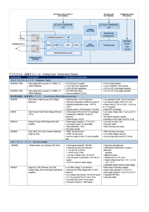
アナログ入力 温度モジュール
アナログ・デバイセズのオートメーション・コントローラ・セグメントの概要
アナログ・デバイセズは、産業用高精度信号計測ソリューションのリーディング・サプライヤです。これらのソリューションは、化
学および医薬品、炭化水素(石油およびガス)、環境(廃水および処理)、オートモーティブなど、幅広い産業の処理および製造プ
ラント、機械の PLC、DCS システムのオートメーション・コントローラ・モジュールに組み込まれています。定評のある産業用アプ
リケーションのシステム知識と、高性能、低消費電力、高集積が特長の包括的な製品ポートフォリオを有するアナログ・デバイセズ
は、オートメーション・コントローラの設計エンジニアにとって重要なパートナーです。
主な課題とシステムの アナログ・デバイセズを オートメーション・
考慮事項 選ぶ理由 コントローラ・アプリケ
ーション
• 高可用性システム • アナログ・デバイセズは、長年 • 深いシステム知識とオートメー • アナログ入力温度モジュール
• 高信頼性、供給期間の延長、 にわたって産業市場のニーズ ション・コントローラの設計サ • アナログ入力絶縁モジュール
組み立ておよび製造コストの に対応してきた、高精度コン イクルを支えてきた長年の実 • アナログ入力チャンネル間
削減 バータおよびシグナル・プロセ 績 絶縁モジュール
• I/O チャンネル密度の向上と ッサ技術のリーダー • 長い製品ライフサイクル、高い • アナログ出力絶縁モジュール
モジュール・ハウジングの小 • アナログ・デバイセズは、現在 信頼性、納期の順守 • アナログ出力チャンネル間
型化により、消費電力の低減 および将来の産業市場のニー 絶縁モジュール
と熱および電力効率の向上を ズに対応するため、中核技術
実現する、より小型で集積化 およびアプリケーション固有の
されたソリューションに対する 製品に継続的に投資
ニーズが増大 • 幅広いモジュール入出力で最
• 機能安全の向上に対するエン も効率的な高精度計測機能を
ド・マーケットのニーズの増大 備えた、クラス最高のシグナ
ル・チェーン・ソリューション
www.analog.com/jp
Page2
ISOLATION
SUPERVISORY
REF
RTD
PROFIBUS
THERMOCOUPLE
ADC DATAISOLATION
TEMPERATURE
アナログ入力(温度モジュール)Analog Input: Temperature Module
Part Number Description Key Features and Benefits
マルチプレクサ/スイッチ / Multiplexer / Switch
ADG5208 / 5209 High voltage latch-up proof, 8:1 (5208) / 4:1 • 8 kV I/O port to supplies • 0.4 pC charge injection
(5209) Multiplexer • 2.9 pF off source capacitance • Low on resistance: 160 Ω typical
• 34 pF off drain capacitance • ±9 V to ±22 V dual-supply operation
ADG5408 / 5409 High voltage latch-up proof, 8:1 (5408) / 4:1 • 8 kV HBM ESD rating • ±9 V to ±22 V dual supply operation
(5409) Multiplexer • Low on resistance (13.5 Ω)
電流源回路部(基準電圧とアンプ)/ Current Source Block (Reference and Amp)
ADR3450 Micro-Power, High-Accuracy 5.0V Voltage • Initial accuracy: ±0.1% (maximum) • Low quiescent current: 100 μA (maximum)
Reference • Maximum temperature coefficient: 8 ppm/°C • Low dropout voltage: 250 mV at 2 mA
• Operating temperature range: −40°C to • Output noise (0.1 Hz to 10 Hz): <10 μV p-p
+125°C at 1.2 V (typical)
• Output current: +10 mA source/−3 mA sink • 6-lead SOT-23 package
ADR550 High Precision Shunt Mode Voltage Reference • Ultracompact SC70 and SOT-23-3 packages • Low output voltage noise: 14 μV p-p @ 2.5
(5.0 V) • Temperature coefficient: 40 ppm/°C V output
maximum) • No external capacitor required
• Initial accuracy: ±0.2% • Operating current range: 50 μA to 15 mA
AD8541/2 General-Purpose CMOS Single Rail-to-Rail • Single-supply operation: 2.7 V to 5.5 V • Low input currents: 4 pA
Amplifier • Low supply current: 45 μA/amplifier • Unity gain stable
• Wide bandwidth: 1 MHz • Rail-to-rail input and output
• No phase reversal
ADA4505 10µA, RRIO, Zero Input Crossover Distortion • PSRR: 100 dB minimum • Rail-to-rail input and output
Single Op Amp • CMRR: 105 dB typical • 3 mV offset voltage maximum
• Very low supply current: 10 μA per amplifier • Very low input bias current: 0.5 pA typ.
max.
ADCドライブ・アンプ / ADC Drive Amplifier
ADA4940 Ultralow Power, Low Distortion ADC Driver • Small signal bandwidth: 260 MHz • Externally adjustable gain
• Extremely low harmonic distortion • Differential-to-differential or single-to-
• −122 dB THD at 50 kHz differential
• −96 dB THD at 1 MHz operation
• Low input voltage noise: 3.9 nV/√Hz • Balanced outputs
• Very low power consumption: 6.25 mW (5 V • Settling time to 0.1%: 34 ns
supply) • Output voltage swing from −VS + 0.1 V to
• 0.35 mV maximum offset voltage +VS − 0.1 V
• Adjustable output common-mode voltage
ADA4522 Single 55 V, EMI Enhanced, Zero-Drift, • Low offset voltage: 5 μV maximum • Wide range of operating voltages
Ultralow Noise, Rail-to-Rail Output Operational • Extremely low offset voltage drift: 22 nV/°C • Single-supply operation: 4.5 V to 55 V
Amplifiers maximum • Dual-supply operation: ±2.25 V to ±27.5 V
• Low voltage noise density: 5.8 nV/√Hz typical • Integrated EMI filters
• 117 nV p-p typical from 0.1 Hz to 10 Hz • Unity-gain stable
• Low input bias current: 50 pA typical
• Unity-gain crossover: 3 MHz typical
Page3
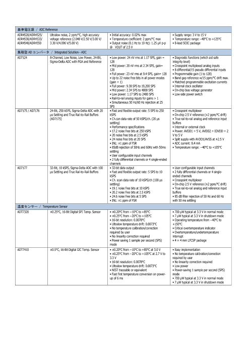
基準電圧源 / ADC Reference
ADR4520/ADR4525/ Ultralow noise, 2 ppm/°C, high accuracy • Initial accuracy: 0.02% max • Supply range: 3 V to 15 V
ADR4530/ADR4533/ voltage reference (2.048 V/2.50 V/3.00 V/ • Temperature coefficient: 2 ppm/°C max • Temperature range: –40°C to +125°C
ADR4540/ADR4550 3.30 V/4.096 V/5.00 V) • Output noise (0.1 Hz to 10 Hz): 1.25 μV p-p • 8-lead SOIC package
@ VOUT of 2.5 V
集積型 ADコンバータ / Integrated Solutiion - ADC
AD7124 8-Channel, Low Noise, Low Power, 24-Bit, • Low power: 24 nV rms at 1.17 SPS, gain = • Diagnostic functions (which aid safe
Sigma-Delta ADC with PGA and Reference 128 integrity level)
• Mid power: 20 nV rms at 2.34 SPS, gain= • Crosspoint multiplexed analog inputs
128 • 8 differential/15 pseudo differential inputs
• Full power: 23 nV rms at 9.4 SPS, gain= 128 • Programmable gain (1 to 128)
• Up to 22 noise free bits in all power modes • Band gap reference w/15 ppm/°C drift max.
(gain = 1) • Matched programmable excitation currents
• Full power: 9.38 SPS to 19,200 SPS • Internal clock oscillator
• Mid power: 2.34 SPS to 4800 SPS • On-chip bias voltage generator
• Low power: 1.17 SPS to 2400 SPS • Low-side power switch
• Rail-to-rail analog inputs for gains > 1
• Simultaneous 50 Hz/60 Hz rejection at 25
SPS
AD7175 / AD7176 24-Bit, 250 kSPS, Sigma-Delta ADC with 20 • Fast and flexible output rate: 5 SPS to 250 • Crosspoint multiplexer
µs Settling and True Rail-to-Rail Buffers kSPS • On-chip 2.5 V reference (±2 ppm/°C drift)
(AD7175) • Ch.can data rate of 50 kSPS/ch. (20 µs • True rail-to-rail analog and reference input
settling) buffers
• Performance specifications • Internal or external clock
• 17.2 noise free bits at 250 kSPS • Power: AVDD1 = 5 V, AVDD2 = IOVDD = 2
• 20 noise free bits at 2.5 kSPS V to 5 V
• 24 noise free bits at 20 SPS • Split supply with AVDD1/AVSS at ±2.5 V
• INL: ±1 ppm of FSR • ADC current: 8.4 mA
• 85dB rejection of 50Hz and 60Hz with 50ms • Temperature range: −40°C to +105°C
settling
• User configurable input channels
• 2 fully differential channels or 4 single-ended
channels
AD7177 32-Bit, 10 kSPS, Sigma-Delta ADC with 100 • 32-bit data output • User configurable input channels
µs Settling and True Rail-to-Rail Buffers • Fast and flexible output rate: 5 SPS to 10 • 2 fully differential channels or 4 single-
kSPS ended channels
• Ch. scan data rate of 10 kSPS/ch (100 µs • Crosspoint multiplexer
settling) • On-chip 2.5 V reference (±2 ppm/°C drift)
• 19.1 noise free bits at 10 kSPS • True rail-to-rail analog and reference input
• 20.2 noise free bits at 2.5 kSPS buffers
• 24.6 noise free bits at 5 SPS • 85 dB filter rejection of 50 Hz and 60 Hz
• INL: ±1 ppm of FSR with 50 ms settling
温度センサー / Temperature Sensor
ADT7320 ±0.25°C, 16-Bit Digital SPI Temp. Sensor • ±0.20°C from −10°C to +85°C • 700 μW typical at 3.3 V in normal mode
• ±0.25°C from −20°C to +105°C • 7 μW typical at 3.3 V in shutdown mode
• 16-bit resolution: 0.0078°C • Operating temperature from −40°C to
• Ultralow temperature drift: 0.0073°C +150°C
• No temperature calibration/correction • Critical overtemperature indicator
required by user • Overtemperature/undertemperature
• No linearity correction required interrupt
• Power saving 1 sample per second (SPS) • 4 × 4 mm LFCSP package
mode
ADT7410 ±0.5°C, 16-Bit Digital I2C Temp. Sensor • ±0.20°C from −10°C to +85°C at 3.0 V • Easy implementation
• ±0.25°C from −20°C to +105°C at 2.7 V to • No temperature calibration/correction
3.3 V required by user
• 16-bit resolution: 0.0078°C • No linearity correction required
• Ultralow temperature drift: 0.0073°C • Low power
• NIST traceable or equivalent • Power-saving 1 sample per second (SPS)
• Fast first temperature conversion on power- mode
up of 6 ms • 700 μW typical at 3.3 V in normal mode
• 7 μW typical at 3.3 V in shutdown mode
Page4
マイコン集積ソリューション / Integrated Solution – Microcontroller
ADuCM361 Low power percision andlog microcontroller, • Analog performance • Power consumption only 1 mA with core
ARM Cortex™-M3 with single Σ-∆ ADCs • Dual PGA and 24-bit, 4 kSPS ADCs operating at 500 kHz (both ADCs on, input
• 12 multiplexed analog inputs buffers off, PGA gain of 4, one SPI port on,
• 12-bit DAC and all timers on)
• Digital performance • Package and temperature
• 32-bit ARM Cortex-M3 processor • 48-lead LFCSP (7 mm × 7 mm)
• 128 kB flash, 8 kB SRAM • –40°C to +125°C
ADuC7061 Low power, precision analog microcontroller, • Dual 24-bit 8 kSPS Σ-∆ ADCs • 32 kB flash and 4 kB SRAM
ARM7TDMI® with single Σ-∆ ADCs • 8 multiplexed analog inputs • UART, SPI, GPIO, PWM
• Single 14-bit DAC • Nominal supply 2.5 V
• ARM7TDMI 16-/32-bit RISC controller • Temperature range: –40°C to +125°C
アイソレーション電源 / Power Isolation
ADuM3471 Quad-channel data with isolated switching • Integrated transformer driver • Quad dc-to-25 Mbps (NRZ) signal isolation
regulators • Regulated adjustable output: 3.3 V to 24 V channels
• 2 W output power • 20-lead SSOP package
• Temperature range: −40°C to +105°C
ADP1621 Constant frequency, current mode step-up • 92% efficiency (no sense resistor required) • Programmable operating frequency
dc-to-dc controller • ±1.0% initial accuracy (100 kHz to 1.5 MHz) with one resistor
• Capable of high supply input voltage (> 5.5 • Synchronizable to external clock
V)
with an external NPN or a resistor
ADuM3190 2.5 kV rms isolated error amplifier • Stable over time and temperature • Low power operation: < 7 mA total
• 0.5% initial accuracy • Wide supply voltage range: 3 V to 20 V
• 1% accuracy over the full temperature range • Temperature range: −40°C to +125°C
• Bandwidth: 400 kHz • 16-lead QSOP package
アイソレーション / Isolation
ADuM140/141/142 D Robust, Quad Channel Isolator W/ Input High common-mode transient immunity: 100 Low dynamic power consumption
Disable kV/μs 1.8 V to 5 V level translation
High robustness to radiated and conducted High temperature operation: 125°C
noise Fail-safe high or low options
Low propagation delay 16-lead, RoHS compliant, SOIC package
13 ns maximum for 5 V operation ADuM140E1/ADuM141E1/ADuM142E1 pin-
15 ns maximum for 1.8 V operation compatible with
150 Mbps maximum guaranteed data rate ADuM1400/ADuM1401/ADuM1402
ADuM140/141/142 E Robust, Quad Channel Isolator W/ Output • High common-mode transient immunity: 100 • Low dynamic power consumption
Enable kV/μs • 1.8 V to 5 V level translation
• High robustness to radiated and conducted • High temperature operation: 125°C
noise • Fail-safe high or low options
• Low propagation delay • 16-lead, RoHS compliant, SOIC package
• 13 ns maximum for 5 V operation • ADuM140D1/ADuM141D1/ADuM142D1 pin-
• 15 ns maximum for 1.8 V operation compatible with
• 150 Mbps maximum guaranteed data rate ADuM1400/ADuM1401/ADuM1402
DC/DCコンバータ / DC / DC Converter
ADP2441 36 V, 1 A, synchronous step-down • Wide input voltage range: 4.5 V to 36 V • Adjustable frequency 300 kHz to 1 MHz
dc-to-dc regulator • Adjustable output down to 0.6 V • Soft start with tracking, power-good pin,
• High efficiency up to 94% and overcurrent limit protection
• ±1% output voltage accuracy
ADP2442 36 V,1 A, Synchronous, Step-Down, DC-to- • Wide input voltage range of 4.5 V to 36 V • External synchronization from 300 kHz to 1
DC Regulator with External Clock • Low minimum on time of 50 ns MHz
Synchronization • Maximum load current of 1 A • Pulse skip mode or Forced fixed frequency
• High efficiency of up to 94% mode
• Adjustable output down to 0.6 V • Precision enable input pin
• ±1% output voltage accuracy • Open-drain power good
• Adjustable switching frequency of 300 kHz to • Reference similar product ADP2441 with
1 MHz programmable soft-start and tracking.
ADP1621 Constant frequency, current mode step-up • 92% efficiency (no sense resistor required) • Programmable operating frequency
dc-to-dc controller • ±1.0% initial accuracy (100 kHz to 1.5 MHz) with one resistor
• Capable of high supply input voltage (> 5.5 • Synchronizable to external clock
V) with an external NPN or a resistor
ADP5050/ADP5051/ Integrated power solution with quad buck • Wide input voltage range: 4.5 V to 15 V • 250 kHz to 1.4 MHz adj. switching
ADP5052/ADP5053 regulators • I2C Interface (ADP5050, ADP5051) frequency
• 200 mA LDO regulator (ADP5050, ADP5052) • Two programmable 1.2 A/2.5 A/4 A sync
• Watchdog timer and reset (ADP5051, buck regulators with low-side FET driver
ADP5053) • Two 1.2 A sync buck regulators
Page5
リニア・レギュレータ / LDO
ADP7182 -200mA, negative voltage input, Low Noise • Low Noise: 18 μV RMS • Low dropout voltage: 185 mV @ -200 mA
• Power supply rejection ratio (PSRR): 66 dB at load
10 KHz at VOUT=-3V • Initial accuracy: ±1%
• Positive or Negative Enable Logic • Accuracy over line, load, and temperature:
• Stable with small 2.2μF ceramic output +2% maximum/−3% minimum
capacitor
• Input voltage range: -2.7 V to -28 V
• Maximum output current: -200 mA
ADP7102/7104/7105 20 V, 300 / 500 mA, Low Noise, CMOS LDO • Input voltage range: 3.3 V to 20 V • Reverse current protection
Maximum output current: 300 mA (ADP7102), • Low dropout voltage:
500 mA (ADP7104/5) • 200 mV at 300 mA load (ADP7102),
Low noise: 15 μV rms for fixed output versions 350 mV at 500mA load (ADP7105)
PSRR performance of 60 dB at 10 kHz, VOUT = • Initial accuracy: ±0.8%
3.3 V
ADP7112 / 7118 20 V, 200 mA, Low Noise, CMOS LDO • Low noise: 11 µV rms independent of fixed • Low dropout voltage: 200 mV (typical) at a
output voltage 200 mA load, VOUT = 5 V
• PSRR of 88 dB at 10 kHz, 68 dB at 100 kHz, • User programmable soft start
50 dB at 1 MHz, VOUT ≤ 5 V, VIN = 7 V • Low quiescent current, IGND = 50 μA
• Input voltage range: 2.7 V to 20 V (typical) with no load
• Maximum output current: 200 mA • 1x1.2, 6-ld WLCSP (ADP7112)
• Initial accuracy: ±0.8% 2x2, 6-ld LFCSP / 8ld-SOIC / 5ld-TSOT
• Accuracy over line, load, and temperature (ADP7118)
±1.8%, TJ = −40°C to +125°C
ADP7142 40 V, 200 mA, Low Noise, CMOS LDO • Low Noise: 11 μVRMS independent of fixed • Low dropout voltage: 200 mV @ 200 mA
output load, VOUT = 5V
• PSRR of 88 dB @ 10 KHz, 68 dB @ 100 KHz, • User programmable Soft Start
50 dB @ 1 MHz, VOUT ≤5V, VIN = 7V (LFCSP and SOIC only)
• Input voltage range: 2.7 V to 40 V • Low Quiescent Current, IGND = 50 μA with
• Maximum output current: 200 mA no load
• Initial accuracy: ±0.8% • Low shutdown current: 1.8 μA @ VIN = 5
• Accuracy over line, load, and temperature V, 3.0 μA @ VIN = 40 V
±1.1%, TJ = −40°C to +85°C • Stable with small 2.2μF ceramic output
±1.8%, TJ = −40°C to +125°C capacitor
コントローラ / Controller
ADSP-BF504/504F Low Cost Blackfin with Optimized Peripheral • 400 MHz (800 MMACS) Blackfin® core • 32 MB executable flash
Set for Industrial and General Purpose • 2 UART, 2 SPI, 2 SPORT, and CAN interfaces (ADSP-BF504F/ADSP-BF506F)
Applications for communications • True 12-bit, dual SAR ADC (ADSP-BF506F)
インターフェース/通信 / Interface / Communication
ADM1486 5 V, High Speed (30 Mbps), Low Power, Half • 30 Mbps Data Rate • 0.5 ns Skew Driver and Receiver
Duplex RS-485 PROFIBUS Transceiver • 2.1 V Minimum Differential Output with 54 Ω • Driver Propagation Delay: 11 ns
Termination • Receiver Propagation Delay: 12 ns
• Low Power 0.8 mA ICC • High Impedance Outputs with Drivers
Disabled or Power Off
ADM2485 / 2486 2.5 kV Signal Isolated, High Speed, Half • 20 Mbps data rate (ADM2486) • Receiver open-circuit, fail-safe design
Duplex RS-485 PROFIBUS Transceiver w/ • 5 V or 3 V operation (VDD1) • 50 nodes on bus
Transformer Driver • High common-mode transient immunity: >25 • Operating temperature range: −40°C to
kV/μs +85°C
• Isolated DE status output • Wide body, 16-lead SOIC package
ADM2482E 2.5 kV Signal Isolated, ESD Protected, • ±15 kV ESD protection on RS485 • True fail-safe receiver inputs
Full/Half Duplex RS-485 Transceiver w/ input/output pins • Operating temperature range: −40°C to
Transformer Driver (16 Mbps) • Data rate: 16 Mbps +85°C
• 5 V or 3.3 V operation (VDD1) • Wide-body, 16-lead SOIC package
• 256 nodes on bus
ADM2490E 5 kV Signal Isolated, High Speed (16 Mbps), • ±8 kV ESD protection on RS-485 input/output • 32 nodes on the bus
ESD Protected, Full Duplex RS-485 pins • Thermal shutdown protection
Transceiver • 16 Mbps data rate • Operating temperature range: −40°C to
• Suitable for 5 V or 3 V operation (VDD1) +105°C
• High common-mode transient immunity: >25 • Wide body, 16-lead SOIC package
kV/μs
• Receiver has open-circuit, fail-safe design
ADM2587E 2.5 kV Signal and Power Isolated, ±15 kV • isoPower™ integrated isolated DC/DC • Connect up to 256 nodes on one bus
ESD Protected, Full/Half Duplex RS-485 converter • Open- and short-circuit, fail-safe receiver
Transceiver (500kbps) • ±15 kV ESD protection on RS485 inputs
input/output pins • High common-mode transient immunity:
• ADM2587E data rate: 500 kbps >25 kV/μs
• 5 V or 3.3V operation • Thermal shutdown protection
Page6
ADM3051 High Speed Industrial CAN Transceiver with • High speed data rates up to 1 Mbps • Unpowered nodes do not disturb the bus
Bus Protection for 24 V Systems • Short-circuit protection on bus pins • Temperature range: −40°C to +125°C
• Slope control for reduced EMI
ADM3052 5 kV rms isolated CAN transceiver with • High speed data rates up to 1 Mbps • Short-circuit protection on bus pins
integrated high voltage, bus side, linear • Fully isolated digital interface • Integrated bus miswire protection
regulator • Integrated V+ linear regulator • Unpowered nodes do not disturb the bus
• Bus side powered by V+ and V−
ADM3053 2.5 kV rms signal and power isolated CAN • High speed data rates up to 1 Mbps • Slope control for reduced EMI
transceiver with integrated isolated dc-to-dc • Fully isolated power and data • Unpowered nodes do not disturb the bus
converter • Short-circuit protection on bus pins
ADM3054 5 kV rms signal isolated high speed CAN • High speed data rates up to 1 Mbps • Unpowered nodes do not disturb the bus
transceiver with bus protection • Fully isolated digital interface • Able to detect loss of power on bus side
• Short-circuit protection on bus pins • Temperature range: −40°C to +125°C
ADM3101E ±15 kV ESD protected, 3.3 V single-channel • 460 kbps data rate • 0.1 μF charge pump capacitors
RS-232 line driver/receiver • Single-channel RS-232 line driver/receiver
ADM3251E / 3252E Isolated Single/Dual Channel RS-232 Line • 460 kbps data rate • 15 kV ESD protection on RIN and TOUT pins
Driver/Receiver • Fully isolated power and data
ADM3232E ±15 kV ESD Protected, 3.3 V, RS-232 Line • Data rate: 460 kbps • ESD protection to IEC1000-4-2 (801.2) on
Driver/Receiver • 2 Tx and 2 Rx TTL/CMOS and RS-232 I/Os
• Meets EIA-232E specifications • Contact discharge: ±8 kV
• 0.1 μF charge pump capacitors • Air gap discharge: ±15 kV
ADM3311E 3-V, RS-232 Serial Port Driver-Receiver • Green Idle power-saving mode • One receiver active in shutdown
• Single 2.7 V to 3.6 V power supply (ADM3307E/ADM3311E/ADM3312E/ADM3315
• 0.1 µF to 1 µF charge pump capacitors E)
• Low EMI • Two receivers active in shutdown
• Low power shutdown: 20 nA (ADM3310E)
• Full RS-232 compliance • ESD >15 kV IEC 1000-4-2 on RS-232 I/Os
• 460 kb/s data rate • ESD >15 kV IEC 1000-4-2 on CMOS and
RS-232 I/Os (ADM3307E)
電源シーケンサ/電圧検出 / Sequencer / Supervisory
ADM1185 Quad Voltage Monitor and Sequencer • Powered from 2.7 V to 5.5 V on the VCC pin • Monitors 4 supplies via 0.8% accurate
• Logical core with internal timeouts provides comparators
power • 3 open-drain enable outputs
supply sequencing and fault protection • Open-drain power-good output (PWRGD)
• 4 inputs can be programmed to monitor • 10-lead MSOP
different voltage levels with resistor dividers
ADM8323 Supervisory Circuit with Windowed • Windowed watchdog, 8 timeout options • Open-Drain or Push-Pull RESET outputs
Watchdog, Manual Reset, and Active-Low • 26 reset threshold options • Low power consumption
Push-Pull Reset Output • 2.5 V to 5 V in 100 mV increments • Specified over wide temp. range (-40°C to
• 4 reset timeout options 125°C)
• 1 ms, 20 ms, 140 ms, and 1120 ms • 5-lead SOT-23 package
(minimum)
• Manual reset input
ADM6306 Multiple Input Programmable Supervisory Ics • Adj. input threshold voltage options: 0.4 V • Reset output stage: active low, open drain
and 1.23 V • Low power consumption: 5 μA typical
• Pre-trimmed VCC threshold options • Power supply glitch immunity
(ADM6306) • 5-lead SOT-23 package
• Increments between 2.5 V and 5 V • Temperature range: −40°C to +125°C
• Manual reset input (ADM6306)
• 4 factory programmed reset timeout delays
1 ms, 20 ms, 140 ms, and 1.12 sec
(minimum)
ADM6326 Ultralow Power, 3-Lead, SOT-23, • Ultralow supply current 1 μA max. • Push-pull RESET (ADM6326/ADM6346)
Microprocessor Reset Circuit, Active-Low (ADM6326/6328) • Open-drain RESET (ADM6328/ADM6348)
Push-Pull Output, 0.5 µA Supply Current • Accurate monitoring of 2.5 V, 3 V, 3.3 V, and • Power-on reset pulse width of 100 ms min.
5 V • Operating temperature range of −40°C to
• Reset thresholds of 2.2 V to 4.63 V +85°C
• Glitch immunity from negative-going VCC • 3-lead SOT-23 package
transients
• Power-on reset pulse width of 100 ms min.
• 2 reset output options
インターフェース IC、LDO、DC/DC コンバータ、シーケンサ・電圧検出 IC は、他にも製品がございます。詳しくは Web をご参照下さい。
Page7
アナログ入力モジュール
ISOLATION
SUPERVISORY
REF
FAULT PROFIBUS
0V TO 5V
ISOLATION
アナログ入力モジュール:チャンネル間絶縁
BACKPLANE COMMUNICATION
24V NOMINAL (FIELDBUS)
POWER
DC-TO-DC CONVERTER
LDO
VOLTAGE INPUT
±10V, ±5V, 0V TO 10V,
0V TO 5V FAULT SEQUENCER
PROTECTION AMP MCU
DATA
CURRENT INPUT
4mA TO 20mA, ±20mA
RS-485
CONTROLLER
CAN
POWER RS-232
VOLTAGE INPUT
±10V, ±5V, 0V TO 10V,
0V TO 5V FAULT DATA
PROTECTION AMP MCU
CURRENT INPUT
4mA TO 20mA, ±20mA
Page8
Part Number Description Key Feaures and Benefits
入力段保護 / Fault Protection
ADG5462F User Defined Fault Protection and • User defined secondary supplies set • Low on resistance: 10 Ω typical
Detection,10 Ω Ron, Quad Channel overvoltage level • On-resistance flatness: 0.5 Ω
Protector • Overvoltage protection up to −55 V maximum
and +55 V • 4 kV human body model (HBM) ESD
• Power-off protection up to −55 V and rating
+55 V • Latch-up immune under any
• Overvoltage detection on source pins circumstance
• Minimum secondary supply level: 4.5 V • ±5 V to ±22 V dual supply operation
single-supply • Fully specified at ±15 V, ±20 V, +12
• Interrupt flag indicates fault status V, and +36 V
入力段アンプ / Amplifier
AD8226 Wide Supply Range, Rail-to-Rail Output • Gain set with 1 external resistor • Bandwidth (G = 1): 1.5 MHz
Instrumentation Amplifier • Gain range: 1 to 1000 • CMRR (G = 1): 90 dB minimum for BR
• Input voltage goes below ground models
• Inputs protected beyond supplies • Input noise: 22 nV/√Hz
• Very wide power supply range • Typical supply current: 350 μA
• 2.2 V to 36 V or ±1.35 V to ±18 V supply • Specified temperature: −40°C to +125°C
AD8421 3 nV /√Hz, Low Power Instrumentation • 2.3 mA maximum supply current • 35 V/µs slew rate
Amplifier • 3.2 nV/√Hz maximum input voltage noise at 1 • High precision dc performance
kHz • 94 dB CMRR minimum (G = 1)
• 200 fA/√Hz current noise at 1 kHz • 0.2 µV/°C maximum input offset voltage
• 10 MHz bandwidth (G = 1) drift
• 2 MHz bandwidth (G = 100) • 1 ppm/°C maximum gain drift (G = 1)
• 0.6 µs settling time to 0.001% (G = 10) • 500 pA maximum input bias current
• 80 dB CMRR to 20 kHz (G = 1)
AD8422 High Performance, Low Power, Rail-to-Rail • 330 μA maximum quiescent current • 150 dB minimum CMRR (G = 1000)
Precision Instrumentation Amplifier • Rail-to-rail output • 0.04% maximum gain error (G = 1000)
• Low noise and distortion • 0.3 μV/°C maximum input offset drift
• 8 nV/√Hz maximum input voltage noise at 1 • 0.5 nA maximum input bias current
kHz • 4.6 V to 36 V or ±2.3 V to ±18 V dual
• 0.15 μV p-p RTI noise (G = 100) supply
• 0.5 ppm nonlinearity with 2 kΩ load (G = 1) • Input overvoltage protection:
• 80 dB minimum CMRR at 10 kHz (G = 1) • Gain range: 1 to 1000
• 2.2 MHz bandwidth (G = 1)
ADA4522 Single 55 V, EMI Enhanced, Zero-Drift, • Low offset voltage: 5 μV maximum • Single-supply operation: input voltage range
Ultralow Noise, Rail-to-Rail Output • Extremely low offset voltage drift: 22 nV/°C includes ground and rail-to-rail output
Operational Amplifiers maximum • Wide range of operating voltages
• Low voltage noise density: • Single-supply operation: 4.5 V to 55 V
• 5.8 nV/√Hz typical • Dual-supply operation: ±2.25 V to ±27.5 V
• 117 nV p-p typical from 0.1 Hz to 10 Hz • Integrated EMI filters
• Low input bias current: 50 pA typical • Unity-gain stable
• Unity-gain crossover: 3 MHz typical
ADA4096-2/4 30V, micropower, overvoltage protection, • Input overvoltage protection, 32V above and • Single-supply operation: 3V to 30V
RRIO, dual/quad OPAMPs below the supply rails • Rail-to-Rail input and output swing
• No phase reversal for input voltage up to ±32V • Unity gain bandwidth: 800kHz typ
beyond the power supply @VSY=±15V
マルチプレクサ・スイッチ / Multiplexer / Switch
ADG5208 / 5209 High voltage latch-up proof, 8:1 (5208) / • 8 kV I/O port to supplies • 0.4 pC charge injection
4:1 (5209) Multiplexer • 2.9 pF off source capacitance • Low on resistance: 160 Ω typical
• 34 pF off drain capacitance • ±9 V to ±22 V dual-supply operation
ADG5408 / 5409 High voltage latch-up proof, 8:1 (5408) / • 8 kV HBM ESD rating • ±9 V to ±22 V dual supply operation
4:1 (5409) Multiplexer • Low on resistance (13.5 Ω)
ADCドライブ・アンプ / ADC Drive Amplifier
AD8275 G=0.2, level translation, 16-bit ADC driver • Translates ±10V to +4V • Low offset drift: 2.5mV//°C
• Drives 16bit SAR ADCs • Rail-to-Rail output
• High CMRR: 96dB • 8-lead MSOP package
• Low gain drift: 1ppm/°C
AD8475 Precision, selectable gain, full differential • Attenuate and level shift: G=0.4x, 0.8x • Suited for driving 18-bit converter up
funnel amp • Fully differential or single-ended to 4MSPS
input/output • 10 nV/√Hz output noise
• Rail-to-Rail output • Low gain drift: 1ppm/°C
Page9
ADA4610 Low Noise, Precision, Rail-to-Rail Output, • Low offset voltage • Low voltage noise: 0.45 μV p-p at
JFET Single Op Amp B grade: 0.4 mV max (ADA4610-1/- 0.1 Hz to 10 Hz
2) • Voltage noise density: 7.30 nV/√Hz
A grade: 1 mV max at f = 1 kHz
• Low offset voltage drift • Low total harmonic distortion (THD)
B grade: 4 μV/°C max (ADA4610-1/- + noise:
2) 0.00025%
A grade: 8 μV/°C max (SOIC, MSOP, • No phase reversal
LFCSP) • Rail-to-rail output
• Low input bias current: 5 pA typical • Unity-gain stable
• Dual-supply operation: ±5 V to ±15 V
Page10
基準電圧源 / Reference
ADR4520/ADR4525/ Ultralow noise, 2 ppm/°C, high accuracy • Initial accuracy: 0.02% max • Supply range: 3 V to 15 V
ADR4530/ADR4533/ voltage reference (2.048 V/2.50 V/3.00 V/ • Temperature coefficient: 2 ppm/°C max • Temperature range: –40°C to
ADR4540/ADR4550 3.30 V/4.096 V/5.00 V) • Output noise (0.1 Hz to 10 Hz): 1.25 +125°C
μV p-p @ VOUT of 2.5 V • 8-lead SOIC package
ユニバーサル I/O / Universal I/O
AD5592R 8 Channel, 12-Bit, Configurable ADC/DAC • 8-channel, configurable ADC/DAC/GPIO • Integrated temperature sensor
with on-chip Reference, SPI interface • Configurable as any combination of • SPI interface
8 × 12-bit DAC channels • 16-ball, 2 mm × 2 mm WLCSP
8 × 12-bit ADC channels • 16-lead, 3 mm × 3 mm LFCSP
8 × general-purpose digital • 16-lead TSSOP
input/output pins
ADコンバータ / ADC
AD7685 16 / 14 bit, 250kSPS PulSAR® ADC • Throughput: 250 kSPS • INL: ±2 LSB max
• Pseudo differential analog input range: • SINAD: 93.5 dB @ 20 kHz
0 V to VREF with VREF up to VDD • Supply range: 2.3 V to 5.5 V
AD7643 18bit 1.2MSPS PulSAR • Throughput: 1.25 MSPS • THD: −112 dB typical @ 20 kHz
• INL: ±2 LSB typ, ±3 LSB max; ±8 ppm (VREF = 2.5 V)
of full scale • 2.048 V internal reference: typ drift
• Dynamic range: 95.5 dB 10 ppm/°C;
• SNR: 93.5 dB typical @ 20 kHz (VREF = TEMP output
2.5 V) • Differential input range: ±VREF
(VREF up to 2.5 V)
集積型 ADコンバータ / Integrated Solution - ADC
AD7124 8-Channel, Low Noise, Low Power, 24-Bit, • Low power: 24 nV rms at 1.17 SPS, • Diagnostic functions (which aid safe
Sigma-Delta ADC with PGA and Reference gain = 128 integrity level)
• Mid power: 20 nV rms at 2.34 SPS, • Crosspoint multiplexed analog inputs
gain= 128 • 8 differential/15 pseudo differential
• Full power: 23 nV rms at 9.4 SPS, inputs
gain= 128 • Programmable gain (1 to 128)
• Up to 22 noise free bits in all power • Band gap reference w/15 ppm/°C
modes (gain = 1) drift max.
• Full power: 9.38 SPS to 19,200 SPS • Matched programmable excitation
• Mid power: 2.34 SPS to 4800 SPS currents
• Low power: 1.17 SPS to 2400 SPS • Internal clock oscillator
• Rail-to-rail inputs for gains > 1 • On-chip bias voltage generator
• Simultaneous 50 Hz/60 Hz rejection at • Low-side power switch
25 SPS
AD7175 / AD7176 24-Bit, 250 kSPS, Sigma-Delta ADC with • Fast and flexible output rate: 5 SPS to • Crosspoint multiplexer
20 µs Settling and True Rail-to-Rail Buffers 250 kSPS • On-chip 2.5 V reference (±2 ppm/°C
(AD7175) • Ch.can data rate of 50 kSPS/ch. (20 µs drift)
settling) • True rail-to-rail analog and reference
• Performance specifications input buffers
• 17.2 noise free bits at 250 kSPS • Internal or external clock
• 20 noise free bits at 2.5 kSPS • Power: AVDD1 = 5 V, AVDD2 =
• 24 noise free bits at 20 SPS IOVDD = 2 V to 5 V
• INL: ±1 ppm of FSR • Split supply with AVDD1/AVSS at
• 85dB rejection of 50Hz and 60Hz with ±2.5 V
50ms settling • ADC current: 8.4 mA
• User configurable input channels • Temperature range: −40°C to
• 2 fully differential channels or 4 single- +105°C
ended channels
HARTモデム / HART modem
AD5700/-1 Low power HART® modem • HART compliant fully integrated FSK • 1.71 V to 5.5 V power supply
modem • Buffered HART output
• On-chip oscillator (AD5700-1) • Temperature range: −40°C to
• 4 mm × 4 mm, 24-lead LFCSP +125°C
Page11
アイソレーション電源 / Power Isolation
ADuM3471 Quad-channel data with isolated switching • Integrated transformer driver • Quad dc-to-25 Mbps (NRZ) signal
regulators • Regulated adjustable output: 3.3 V to isolation
24 V channels
• 2 W output power • 20-lead SSOP package
• Temperature range: −40°C to
+105°C
ADP1621 Constant frequency, current mode step- • 92% efficiency (no sense resistor • Programmable operating frequency
up dc-to-dc controller required) (100 kHz to 1.5 MHz) with one resistor
• ±1.0% initial accuracy • Synchronizable to external clock
• Capable of high supply input voltage (>
5.5 V) with an external NPN or a resistor
ADuM3190 2.5 kV rms isolated error amplifier • Stable over time and temperature • Low power operation: < 7 mA total
• 0.5% initial accuracy • Wide supply voltage range: 3 V to 20
• 1% accuracy over the full temperature V
range • Temperature range: −40°C to
• Bandwidth: 400 kHz +125°C
• 16-lead QSOP package
アイソレーション / Isolation
ADuM140/141/142 D Robust, Quad Channel Isolator W/ Input • High common-mode transient • Low dynamic power consumption
Disable immunity: 100 kV/μs • 1.8 V to 5 V level translation
• High robustness to radiated and • High temperature operation: 125°C
conducted noise • Fail-safe high or low options
• Low propagation delay • 16-lead, RoHS compliant, SOIC
• 13 ns maximum for 5 V operation package
• 15 ns maximum for 1.8 V operation •
• 150 Mbps maximum guaranteed data ADuM140E1/ADuM141E1/ADuM142E1
rate pin-compatible with ADuM1400 /
ADuM1401 / ADuM1402
ADuM140/141/142 E Robust, Quad Channel Isolator W/ Output • High common-mode transient • Low dynamic power consumption
Enable immunity: 100 kV/μs • 1.8 V to 5 V level translation
• High robustness to radiated and • High temperature operation: 125°C
conducted noise • Fail-safe high or low options
• Low propagation delay • 16-lead, RoHS compliant, SOIC
• 13 ns maximum for 5 V operation package
• 15 ns maximum for 1.8 V operation •
• 150 Mbps maximum guaranteed data ADuM140D1/ADuM141D1/ADuM142D1
rate pin-
compatible with
ADuM1400/ADuM1401/ADuM1402
集積 DC / DCコンバータ / DC / DC Converter
ADP2441 36 V, 1 A, synchronous step-down • Wide input voltage range: 4.5 V to 36 V • Adjustable frequency 300 kHz to 1
dc-to-dc regulator • Adjustable output down to 0.6 V MHz
• High efficiency up to 94% • Soft start with tracking, power-good
• ±1% output voltage accuracy pin, and
overcurrent limit protection
ADP2442 36 V,1 A, Synchronous, Step-Down, DC- • Wide input voltage range of 4.5 V to 36 • External synchronization from 300
to-DC Regulator with External Clock V kHz to 1 MHz
Synchronization • Low minimum on time of 50ns ns • Pulse skip mode or Forced fixed
• Maximum load current of 1 A frequency mode
• High efficiency of up to 94% • Precision enable input pin
• Adjustable output down to 0.6 V • Open-drain power good
• ±1% output voltage accuracy • Reference similar product ADP2441
• Adjustable switching frequency of 300 with
kHz to 1 MHz programmable soft-start and
tracking.
ADP1621 Constant frequency, current mode step-up • 92% efficiency (no sense resistor • Programmable operating frequency
dc-to-dc controller required) (100 kHz to 1.5 MHz) with one
• ±1.0% initial accuracy resistor
• Capable of high supply input voltage (> • Synchronizable to external clock
5.5 V) with an external NPN or a resistor
ADP5050/ADP5051/ Integrated power solution with quad buck • Wide input voltage range: 4.5 V to 15 V • 250 kHz to 1.4 MHz adj. switching
ADP5052/ADP5053 regulators • I2C Interface (ADP5050, ADP5051) frequency
• 200 mA LDO regulator (ADP5050, • Two programmable 1.2 A/2.5 A/4 A
ADP5052) sync buck
• Watchdog timer and reset (ADP5051, regulators with low-side FET driver
ADP5053) • Two 1.2 A sync buck regulators
Page12
リニア・レギュレータ / LDO
ADP7182 -200mA, negative voltage input, Low Noise • Low Noise: 18 μV RMS • Low dropout voltage: 185 mV @ -200 mA
• Power supply rejection ratio load
(PSRR): 66 dB at 10 KHz at • Initial accuracy: ±1%
VOUT=-3V • Accuracy over line, load, and temperature:
• Positive or Negative Enable +2% maximum/−3% minimum
Logic
• Stable with small 2.2μF
ceramic output capacitor
• Input voltage range: -2.7 V
to -28 V
• Maximum output current: -
200 mA
ADP7102/7104/7105 20 V, 300 / 500 mA, Low Noise, CMOS LDO • Input voltage range: 3.3 V to • Reverse current protection
20 V • Low dropout voltage:
• Maximum output current: • 200 mV at 300 mA load (ADP7102),
300 mA (ADP7102), 500 mA 350 mV at 500mA load (ADP7105)
(ADP7104/5) • Initial accuracy: ±0.8%
• Low noise: 15 μV rms for
fixed output versions
• PSRR performance of 60 dB
at 10 kHz, VOUT = 3.3 V
ADP7112 / 7118 20 V, 200 mA, Low Noise, CMOS LDO • Low noise: 11 µV rms • Low dropout voltage: 200 mV (typical) at a
independent of fixed output 200 mA load, VOUT = 5 V
voltage • User programmable soft start
• PSRR of 88 dB at 10 kHz, 68 • Low quiescent current, IGND = 50 μA
dB at 100 kHz, 50 dB at 1 (typical) with no load
MHz, VOUT ≤ 5 V, VIN = 7 V • 1x1.2, 6-ld WLCSP (ADP7112)
• Input voltage range: 2.7 V to 2x2, 6-ld LFCSP / 8ld-SOIC / 5ld-TSOT
20 V (ADP7118)
• Maximum output current:
200 mA
• Initial accuracy: ±0.8%
• Accuracy over line, load, and
temperature ±1.8%, TJ =
−40°C to +125°C
ADP7142 40 V, 200 mA, Low Noise, CMOS LDO • Low Noise: 11 μVRMS • Low dropout voltage: 200 mV @ 200 mA
independent of fixed output load,
• PSRR of 88 dB @ 10 KHz, 68 VOUT = 5V
dB @ 100 KHz, 50 dB @ 1 • User programmable Soft Start
MHz, VOUT ≤5V, VIN = 7V (LFCSP and SOIC only)
• Input voltage range: 2.7 V to • Low Quiescent Current, IGND = 50 μA with
40 V no load
• Maximum output current: • Low shutdown current: 1.8 μA @ VIN = 5 V,
200 mA 3.0 μA @ VIN = 40 V
• Initial accuracy: ±0.8% • Stable with small 2.2μF ceramic output
• Accuracy over line, load, and capacitor
temperature
±1.1%, TJ = −40°C to
+85°C
±1.8%, TJ = −40°C to
+125°C
コントローラ / Controller
ADSP-BF504/504F Low Cost Blackfin with Optimized Peripheral • 400 MHz (800 MMACS) Blackfin® • 32 MB executable flash
Set for Industrial and General Purpose core (ADSP-BF504F/ADSP-BF506F)
Applications • 2 UART, 2 SPI, 2 SPORT, and CAN • True 12-bit, dual SAR ADC (ADSP-BF506F)
interfaces for communications
インターフェース/通信 / Interface / Communication
ADM1486 5 V, High Speed (30 Mbps), Low Power, Half • 30 Mbps Data Rate • 0.5 ns Skew Driver and Receiver
Duplex RS-485 PROFIBUS Transceiver • 2.1 V Minimum Differential Output • Driver Propagation Delay: 11 ns
with 54 Ω Termination • Receiver Propagation Delay: 12 ns
• Low Power 0.8 mA ICC • High Impedance Outputs with Drivers Disabled or
Power Off
ADM2485 / 2486 2.5 kV Signal Isolated, High Speed, Half • 20 Mbps data rate (ADM2486) • Receiver open-circuit, fail-safe design
Duplex RS-485 PROFIBUS Transceiver w/ • 5 V or 3 V operation (VDD1) • 50 nodes on bus
Transformer Driver • High common-mode transient • Operating temperature range: −40°C to +85°C
immunity: >25 kV/μs • Wide body, 16-lead SOIC package
• Isolated DE status output
Page13
ADM2482E 2.5 kV Signal Isolated, ESD Protected, • ±15 kV ESD protection on RS485 • True fail-safe receiver inputs
Full/Half Duplex RS-485 Transceiver w/ input/output pins • Operating temperature range: −40°C to +85°C
Transformer Driver (16 Mbps) • Data rate: 16 Mbps • Wide-body, 16-lead SOIC package
• 5 V or 3.3 V operation (VDD1)
• 256 nodes on bus
ADM2490E 5 kV Signal Isolated, High Speed (16 Mbps), • ±8 kV ESD protection on RS-485 • 32 nodes on the bus
ESD Protected, Full Duplex RS-485 input/output pins • Thermal shutdown protection
Transceiver • 16 Mbps data rate • Operating temperature range: −40°C to +105°C
• Suitable for 5 V or 3 V operation • Wide body, 16-lead SOIC package
(VDD1)
• High common-mode transient
immunity: >25 kV/μs
• Receiver has open-circuit, fail-safe
design
ADM2587E 2.5 kV Signal and Power Isolated, ±15 kV • isoPower™ integrated isolated • Connect up to 256 nodes on one bus
ESD Protected, Full/Half Duplex RS-485 DC/DC converter • Open- and short-circuit, fail-safe receiver inputs
Transceiver (500kbps) • ±15 kV ESD protection on RS485 • High common-mode transient immunity: >25 kV/μs
input/output pins • Thermal shutdown protection
• ADM2587E data rate: 500 kbps
• 5 V or 3.3V operation
ADM3051 High Speed Industrial CAN Transceiver with • High speed data rates up to 1 • Unpowered nodes do not disturb the bus
Bus Protection for 24 V Systems Mbps • Temperature range: −40°C to +125°C
• Short-circuit protection on bus pins
• Slope control for reduced EMI
ADM3052 5 kV rms isolated CAN transceiver with • High speed data rates up to 1 • Short-circuit protection on bus pins
integrated high voltage, bus side, linear Mbps • Integrated bus miswire protection
regulator • Fully isolated digital interface • Unpowered nodes do not disturb the bus
• Integrated V+ linear regulator
• Bus side powered by V+ and V−
ADM3053 2.5 kV rms signal and power isolated CAN • High speed data rates up to 1 • Slope control for reduced EMI
transceiver with integrated isolated dc-to-dc Mbps • Unpowered nodes do not disturb the bus
converter • Fully isolated power and data
• Short-circuit protection on bus pins
ADM3054 5 kV rms signal isolated high speed CAN • High speed data rates up to 1 • Unpowered nodes do not disturb the bus
transceiver with bus protection Mbps • Able to detect loss of power on bus side
• Fully isolated digital interface • Temperature range: −40°C to +125°C
• Short-circuit protection on bus pins
ADM3101E ±15 kV ESD protected, 3.3 V single-channel • 460 kbps data rate • 0.1 μF charge pump capacitors
RS-232 line driver/receiver • Single-channel RS-232 line driver /
receiver
ADM3251E / 3252E Isolated Single/Dual Channel RS-232 Line • 460 kbps data rate • 15 kV ESD protection on RIN and TOUT pins
Driver/Receiver • Fully isolated power and data
ADM3232E ±15 kV ESD Protected, 3.3 V, RS-232 Line • Data rate: 460 kbps • ESD protection to IEC1000-4-2 (801.2) on
Driver/Receiver • 2 Tx and 2 Rx TTL/CMOS and RS-232 I/Os
• Meets EIA-232E specifications • Contact discharge: ±8 kV
• 0.1 μF charge pump capacitors • Air gap discharge: ±15 kV
ADM3311E 3-V, RS-232 Serial Port Driver-Receiver • Green Idle power-saving mode • One receiver active in shutdown
• Single 2.7 V to 3.6 V power supply (ADM3307E / ADM3311E / ADM3312E / ADM3315E)
• 0.1 µF to 1 µF charge pump • Two receivers active in shutdown (ADM3310E)
capacitors • ESD >15 kV IEC 1000-4-2 on RS-232 I/Os
• Low EMI • ESD >15 kV IEC 1000-4-2 on CMOS and
• Low power shutdown: 20 nA RS-232 I/Os (ADM3307E)
• Full RS-232 compliance
• 460 kb/s data rate
電源シーケンサ/電圧検出 / Sequencer / Supervisory
ADM1185 Quad Voltage Monitor and Sequencer • Powered from 2.7 V to 5.5 V on • Monitors 4 supplies via 0.8% accurate comparators
the VCC pin • 3 open-drain enable outputs
• Logical core with internal timeouts • Open-drain power-good output (PWRGD)
provides power supply sequencing • 10-lead MSOP
and fault protection
• 4 inputs can be programmed to
monitor different voltage levels with
resistor dividers
ADM8323 Supervisory Circuit with Windowed • Windowed watchdog, 8 timeout • Open-Drain or Push-Pull RESET outputs
Watchdog, Manual Reset, and Active-Low options • Low power consumption
Push-Pull Reset Output • 26 reset threshold options • Specified over wide temp. range (-40°C to 125°C)
• 2.5 V to 5 V in 100 mV increments • 5-lead SOT-23 package
• 4 reset timeout options
• 1 ms, 20 ms, 140 ms, and 1120
ms min
• Manual reset input
Page14
ADM6306 Multiple Input Programmable Supervisory • Adj. input threshold voltage • Reset output stage: active low, open drain
ICs options: 0.4 V and 1.23 V • Low power consumption: 5 μA typical
• Pre-trimmed VCC threshold options • Power supply glitch immunity
(ADM6306) • 5-lead SOT-23 package
• Increments between 2.5 V and 5 V • Temperature range: −40°C to +125°C
• Manual reset input (ADM6306)
• 4 factory programmed reset
timeout delays
1 ms, 20 ms, 140 ms, and 1.12
sec min
ADM6326 Ultralow Power, 3-Lead, SOT-23, • Ultralow supply current 1 μA max. • Push-pull RESET (ADM6326/ADM6346)
Microprocessor Reset Circuit, Active-Low (ADM6326/6328) • Open-drain RESET (ADM6328/ADM6348)
Push-Pull Output, 0.5 µA Supply Current • Accurate monitoring of 2.5 V, 3 V, • Power-on reset pulse width of 100 ms min.
3.3 V, and 5 V • Operating temperature range of −40°C to +85°C
• Reset thresholds of 2.2 V to 4.63 V • 3-lead SOT-23 package
• Glitch immunity from negative-
going VCC transients
• Power-on reset pulse width of 100
ms min.
• 2 reset output options
インターフェース IC、LDO、DC/DC コンバータ、シーケンサ・電圧検出 IC は、他にも製品がございます。詳しくは Web をご参照下さい。
Page15
アナログ出力モジュール
COMMUNICATION BACKPLANE OPTIONAL FIELD SUPPLY
(FIELDBUS) 24V NOMINAL 24V NOMINAL
DC-TO-DC CONVERTER POWER DC-TO-DC CONVERTER
LDO MODEM LDO
ERROR
SEQUENCER AMP
PROTECTION
AMP
OUTPUT
PROTECTION ±10V, ±5V, 0V TO 10V,0V TO 5V
RS-485
DATA
CAN
RS-232 AMP
OUTPUT CURRENT OUTPUTS
PROTECTION 4mA TO 20mA, ±20mA
AMP OUTPUT
アナログ出力モジュール:チャンネル間絶縁
COMMUNICATION BACKPLANE
(FIELDBUS) 24V NOMINAL
DC-TO-DC CONVERTER
LDO POWER
±10V, ±5V, 0V TO 10V,
OUTPUT 0V TO 5VAMP
DATA
CURRENT OUTPUT
SEQUENCER 4mA TO 20mA, ±20mA
HART
MODEM
RS-485
CAN
RS-232
POWER
±10V, ±5V, 0V TO 10V,
OUTPUT 0V TO 5V AMP
DATA
CURRENT OUTPUT
4mA TO 20mA, ±20mA
HART
MODEM
Page16
Part Number Description Key Feaures and Benefits
HARTモデム / HART modem
AD5700/-1 Low power HART® modem • HART compliant fully integrated FSK modem • 1.71 V to 5.5 V power supply
• On-chip oscillator (AD5700-1) • Buffered HART output
• 4 mm × 4 mm, 24-lead LFCSP • Temperature range: −40°C to +125°C
ユニバーサル I/O / Universal I/O
AD5592R 8 Channel, 12-Bit, Configurable • 8-channel, configurable ADC/DAC/GPIO • Integrated temperature sensor
ADC/DAC with on-chip Reference, SPI • Configurable as any combination of • SPI interface
interface 8 × 12-bit DAC channels • 16-ball, 2 mm × 2 mm WLCSP
8 × 12-bit ADC channels • 16-lead, 3 mm × 3 mm LFCSP
8 × general-purpose digital input/output pins • 16-lead TSSOP
DAコンバータ / DAC
AD5681R / AD5683R Single/dual/quad, 16-/12-bit nano • Single (AD5683R / AD5681R), dual (AD5689R / • Offset error: ±1.5 mV max
/ AD5687R / DAC+™ AD5687R), or quad (AD5686R / AD5684R) • 1.8 V logic compatibility
AD5689R / AD5686R with 2 ppm/°C on-chip reference • 12-/16-bit resolution • 8-lead LFCSP (2 mm × 2 mm) or MSOP
/ AD5684R • INL: ±2 LSB maximum @ 16 bits (single)
• On-chip 2.5 V, 5 ppm/°C max reference • 16-lead LFCSP (3 mm × 3 mm) or TSSOP
• Total unadjusted error (TUE): ±0.1% of FSR (dual/quad)
max (±0.06% FSR for single)
アンプ/ 4-20mA 出力アンプ / Amplifier / 4-20mA driver
ADA4077-1/-2/-4 30V, 4 MHz, 7 nV/√Hz, Low Offset and • Low offset voltage: • Low input bias current: <1.0 nA max.
Drift, High Precision Amplifier B-Grade: 25 μV max (SOIC) • Low voltage noise density: 7 nV/√Hz typ at f
A-Grade: 50 μV max (SOIC) = 1 kHz
A-Grade: 120 μV max (MSOP) • CMRR, PSRR, and Avo >120 dB min
• Low offset voltage drift: • Low supply current: 400 μA per amplifier typ
B-Grade: 0.25 μV/°C max (SOIC) • Wide Bandwidth: 4 MHz typ
A-Grade: 0.55 μV/°C max (SOIC) • Dual-supply operation: ±2.5 V to ±15 V
A-Grade: 1.2 μV/°C max (MSOP) • Unity gain stable
• No phase reversal
ADA4177-1 / -2 / -4 OVP and EMI Protected, Precision, Low • Low offset voltage: 60 µV maximum at 25°C • Input overvoltage protection to 32 V above
Noise and Bias Current Single Op Amp (8-lead and 14-lead SOIC) and below the supply voltage rail
• Low offset voltage drift: 1 µV/°C maximum • Integrated EMI filter
(8-lead and 14-lead SOIC) • 70 dB typical rejection at 1000 MHz
• Low input bias current: 1 nA maximum at 25°C • 90 dB typical rejection at 2400 MHz
• Low voltage noise density: 8 nV/√Hz typical at • Rail-to-rail output swing
1 kHz • Low supply current: 500 µA typical per
mplifier
基準電圧源 / Reference
ADR4520/ADR4525/ Ultralow noise, 2 ppm/°C, high accuracy • Initial accuracy: 0.02% max • Supply range: 3 V to 15 V
ADR4530/ADR4533/ voltage reference (2.048 V/2.50 V/3.00 • Temperature coefficient: 2 ppm/°C max • Temperature range: –40°C to +125°C
ADR4540/ADR4550 V/ • Output noise (0.1 Hz to 10 Hz): 1.25 μV p-p @ • 8-lead SOIC package
3.30 V/4.096 V/5.00 V) VOUT of 2.5 V
集積ソリューション / Integrated Solution
AD5750/AD5751/ Industrial current/voltage output • Standard industrial voltage and current output • 60 V/55 V loop compliance (AD5751,
AD5748/AD5749 driver with programmable ranges ranges (including ±20 mA) AD5749)
• Current output only version available (AD5749) • On-chip diagnostics
• ±0.1% FSR max total unadjusted error (TUE) • Temperature range: –40°C to +105°C
on voltage outputs • 32-lead LFCSP package (5 mm × 5 mm)
• ±0.1% FSR max total unadjusted error (TUE)
on current outputs
AD5735 / AD5737 / Quad-channel,16-bit, 4 mA to 20 mA and • Dynamic power control for thermal • ±0.05% FSR max total unadjusted error
AD5757 / AD5755-1 / voltage output DAC, dynamic power management (TUE) on current outputs
AD5755 control, HART connectivity • 16-bit (AD5755-1, AD5755) and 12-bit • Current output only versions available
(AD5735) options (AD5757/AD5737)
• Quad channel • User programmable offset and gain
• Standard industrial voltage and current • On-chip diagnostics
output ranges • On-chip reference (±10 ppm/°C maximum)
• ±0.04% FSR max total unadjusted error • −40°C to +105°C temperature range
(TUE) on voltage outputs • 64-lead LFCSP package (9 mm × 9 mm)
AD5422/AD5412 Single-channel, 12-/16-bit, current • 16-bit (AD5422) and 12-bit (AD5412) options • Current output only versions available
source and voltage output DAC, HART • Standard industrial voltage and current (AD5420/AD5410)
connectivity output ranges • On-chip reference (±10 ppm/°C maximum)
• ±0.1% FSR max total unadjusted error (TUE) • Optional regulated DVCC output
on voltage outputs • 40-lead LFCSP package (6 mm × 6 mm)
• ±0.15% FSR max total unadjusted error (TUE)
on current outputs
Page17
アイソレーション電源 / Power Isolation
ADuM3471 Quad-channel data with isolated switching • Integrated transformer driver • Quad dc-to-25 Mbps (NRZ) signal isolation
regulators • Regulated adjustable output: 3.3 V to 24 channels
V • 20-lead SSOP package
• 2 W output power • Temperature range: −40°C to +105°C
ADP1621 Constant frequency, current mode step-up • 92% efficiency (no sense resistor • Programmable operating frequency
dc-to-dc controller required) (100 kHz to 1.5 MHz) with one resistor
• ±1.0% initial accuracy • Synchronizable to external clock
• Capable of high supply input voltage (>
5.5 V)
with an external NPN or a resistor
ADuM3190 2.5 kV rms isolated error amplifier • Stable over time and temperature • Low power operation: < 7 mA total
• 0.5% initial accuracy • Wide supply voltage range: 3 V to 20 V
• 1% accuracy over the full temperature • Temperature range: −40°C to +125°C
range • 16-lead QSOP package
• Bandwidth: 400 kHz
アイソレーション / Isolation
ADuM140/141/142 D Robust, Quad Channel Isolator W/ Input • High common-mode transient immunity: • Low dynamic power consumption
Disable 100 kV/μs • 1.8 V to 5 V level translation
• High robustness to radiated and • High temperature operation: 125°C
conducted noise • Fail-safe high or low options
• Low propagation delay • 16-lead, RoHS compliant, SOIC package
• 13 ns maximum for 5 V operation • ADuM140E1/ADuM141E1/ADuM142E1 pin-
• 15 ns maximum for 1.8 V operation compatible with ADuM1400 / ADuM1401 /
• 150 Mbps maximum guaranteed data ADuM1402
rate
ADuM140/141/142 E Robust, Quad Channel Isolator W/ Output • High common-mode transient immunity: • Low dynamic power consumption
Enable 100 kV/μs • 1.8 V to 5 V level translation
• High robustness to radiated and • High temperature operation: 125°C
conducted noise • Fail-safe high or low options
• Low propagation delay • 16-lead, RoHS compliant, SOIC package
• 13 ns maximum for 5 V operation • ADuM140D1/ADuM141D1/ADuM142D1 pin-
• 15 ns maximum for 1.8 V operation compatible with
• 150 Mbps maximum guaranteed data ADuM1400/ADuM1401/ADuM1402
rate
DC / DCコンバータ / DC / DC Converter
ADP2441 36 V, 1 A, synchronous step-down • Wide input voltage range: 4.5 V to 36 V • Adjustable frequency 300 kHz to 1 MHz
dc-to-dc regulator • Adjustable output down to 0.6 V • Soft start with tracking, power-good pin, and
• High efficiency up to 94% overcurrent limit protection
• ±1% output voltage accuracy
ADP2442 36 V,1 A, Synchronous, Step-Down, DC-to- • Wide input voltage range of 4.5 V to 36 V • External synchronization from 300 kHz to 1 MHz
DC Regulator with External Clock • Low minimum on time of 50 ns • Pulse skip mode or Forced fixed frequency
Synchronization • Maximum load current of 1 A mode
• High efficiency of up to 94% • Precision enable input pin
• Adjustable output down to 0.6 V • Open-drain power good
• ±1% output voltage accuracy • Reference similar product ADP2441 with
• Adjustable switching frequency of 300 programmable soft-start and tracking.
kHz to 1 MHz
ADP1621 Constant frequency, current mode step-up • 92% efficiency (no sense resistor • Programmable operating frequency
dc-to-dc controller required) (100 kHz to 1.5 MHz) with one resistor
• ±1.0% initial accuracy • Synchronizable to external clock
• Capable of high supply input voltage (>
5.5 V)
with an external NPN or a resistor
ADP5050/ADP5051/ Integrated power solution with quad buck • Wide input voltage range: 4.5 V to 15 V • 250 kHz to 1.4 MHz adj. switching frequency
ADP5052/ADP5053 regulators • I2C Interface (ADP5050, ADP5051) • Two programmable 1.2 A/2.5 A/4 A sync buck
• 200 mA LDO regulator (ADP5050, regulators with low-side FET driver
ADP5052) • Two 1.2 A sync buck regulators
• Watchdog timer and reset (ADP5051,
ADP5053)
リニア・レギュレータ / LDO
ADP7182 -200mA, negative voltage input, Low Noise • Low Noise: 18 μV RMS • Low dropout voltage: 185 mV @ -200 mA load
• Power supply rejection ratio (PSRR): 66 • Initial accuracy: ±1%
dB at • Accuracy over line, load, and temperature:
10 KHz at VOUT=-3V +2% maximum/−3% minimum
• Positive or Negative Enable Logic
• Stable with small 2.2μF ceramic output
capacitor
• Input voltage range: -2.7 V to -28 V
• Maximum output current: -200 mA
Page18
ADP7102/7104/7105 20 V, 300 / 500 mA, Low Noise, CMOS LDO • Input voltage range: 3.3 V to 20 V • Reverse current protection
Maximum output current: 300 mA • Low dropout voltage:
(ADP7102), 500 mA (ADP7104/5) • 200 mV at 300 mA load (ADP7102),
Low noise: 15 μV rms for fixed output 350 mV at 500mA load (ADP7105)
versions • Initial accuracy: ±0.8%
PSRR performance of 60 dB at 10 kHz,
VOUT = 3.3 V
ADP7112 / 7118 20 V, 200 mA, Low Noise, CMOS LDO • Low noise: 11 µV rms independent of • Low dropout voltage: 200 mV (typical) at a 200
fixed output voltage mA load, VOUT = 5 V
• PSRR of 88 dB at 10 kHz, 68 dB at 100 • User programmable soft start
kHz, 50 dB at 1 MHz, VOUT ≤ 5 V, VIN = 7 • Low quiescent current, IGND = 50 μA (typical)
V with no load
• Input voltage range: 2.7 V to 20 V • 1x1.2, 6-ld WLCSP (ADP7112)
• Maximum output current: 200 mA 2x2, 6-ld LFCSP / 8ld-SOIC / 5ld-TSOT
• Initial accuracy: ±0.8% (ADP7118)
• Accuracy over line, load, and
temperature ±1.8%, TJ = −40°C to
+125°C
ADP7142 40 V, 200 mA, Low Noise, CMOS LDO • Low Noise: 11 μVRMS independent of • Low dropout voltage: 200 mV @ 200 mA load,
fixed output VOUT = 5V
• PSRR of 88 dB @ 10 KHz, 68 dB @ 100 • User programmable Soft Start
KHz, (LFCSP and SOIC only)
50 dB @ 1 MHz, VOUT ≤5V, VIN = 7V • Low Quiescent Current, IGND = 50 μA with no
• Input voltage range: 2.7 V to 40 V load
• Maximum output current: 200 mA • Low shutdown current: 1.8 μA @ VIN = 5 V,
• Initial accuracy: ±0.8% 3.0 μA @ VIN = 40 V
• Accuracy over line, load, and • Stable with small 2.2μF ceramic output
temperature capacitor
±1.1%, TJ = −40°C to +85°C
±1.8%, TJ = −40°C to +125°C
インターフェース通信 / Interface / Communication
ADM1486 5 V, High Speed (30 Mbps), Low Power, • 30 Mbps Data Rate • 0.5 ns Skew Driver and Receiver
Half Duplex RS-485 PROFIBUS Transceiver • 2.1 V Minimum Differential Output with • Driver Propagation Delay: 11 ns
54 Ω • Receiver Propagation Delay: 12 ns
Termination • High Impedance Outputs with Drivers Disabled
• Low Power 0.8 mA ICC or Power Off
ADM2485 / 2486 2.5 kV Signal Isolated, High Speed, Half • 20 Mbps data rate (ADM2486) • Receiver open-circuit, fail-safe design
Duplex RS-485 PROFIBUS Transceiver w/ • 5 V or 3 V operation (VDD1) • 50 nodes on bus
Transformer Driver • High common-mode transient immunity: • Operating temperature range: −40°C to +85°C
>25 kV/μs • Wide body, 16-lead SOIC package
• Isolated DE status output
ADM2482E 2.5 kV Signal Isolated, ESD Protected, • ±15 kV ESD protection on RS485 • True fail-safe receiver inputs
Full/Half Duplex RS-485 Transceiver w/ input/output pins • Operating temperature range: −40°C to +85°C
Transformer Driver (16 Mbps) • Data rate: 16 Mbps • Wide-body, 16-lead SOIC package
• 5 V or 3.3 V operation (VDD1)
• 256 nodes on bus
ADM2490E 5 kV Signal Isolated, High Speed (16 • ±8 kV ESD protection on RS-485 • 32 nodes on the bus
Mbps), ESD Protected, Full Duplex RS-485 input/output pins • Thermal shutdown protection
Transceiver • 16 Mbps data rate • Operating temperature range: −40°C to
• Suitable for 5 V or 3 V operation (VDD1) +105°C
• High common-mode transient immunity: • Wide body, 16-lead SOIC package
>25 kV/μs
• Receiver has open-circuit, fail-safe design
ADM2587E 2.5 kV Signal and Power Isolated, ±15 kV • isoPower™ integrated isolated DC/DC • Connect up to 256 nodes on one bus
ESD Protected, Full/Half Duplex RS-485 converter • Open- and short-circuit, fail-safe receiver inputs
Transceiver (500kbps) • ±15 kV ESD protection on RS485 • High common-mode transient immunity: >25
input/output pins kV/μs
• ADM2587E data rate: 500 kbps • Thermal shutdown protection
• 5 V or 3.3V operation
ADM3051 High Speed Industrial CAN Transceiver with • High speed data rates up to 1 Mbps • Unpowered nodes do not disturb the bus
Bus Protection for 24 V Systems • Short-circuit protection on bus pins • Temperature range: −40°C to +125°C
• Slope control for reduced EMI
ADM3052 5 kV rms isolated CAN transceiver with • High speed data rates up to 1 Mbps • Short-circuit protection on bus pins
integrated high voltage, bus side, linear • Fully isolated digital interface • Integrated bus miswire protection
regulator • Integrated V+ linear regulator • Unpowered nodes do not disturb the bus
• Bus side powered by V+ and V−
ADM3053 2.5 kV rms signal and power isolated CAN • High speed data rates up to 1 Mbps • Slope control for reduced EMI
transceiver with integrated isolated dc-to- • Fully isolated power and data • Unpowered nodes do not disturb the bus
dc converter • Short-circuit protection on bus pins
ADM3054 5 kV rms signal isolated high speed CAN • High speed data rates up to 1 Mbps • Unpowered nodes do not disturb the bus
transceiver with bus protection • Fully isolated digital interface • Able to detect loss of power on bus side
• Short-circuit protection on bus pins • Temperature range: −40°C to +125°C
Page19
ADM3101E ±15 kV ESD protected, 3.3 V single- • 460 kbps data rate • 0.1 μF charge pump capacitors
channel RS-232 line driver/receiver • Single-channel RS-232 line
driver/receiver
ADM3251E / 3252E Isolated Single/Dual Channel RS-232 Line • 460 kbps data rate • 15 kV ESD protection on RIN and TOUT pins
Driver/Receiver • Fully isolated power and data
ADM3232E ±15 kV ESD Protected, 3.3 V, RS-232 Line • Data rate: 460 kbps • ESD protection to IEC1000-4-2 (801.2) on
Driver/Receiver • 2 Tx and 2 Rx TTL/CMOS and RS-232 I/Os
• Meets EIA-232E specifications • Contact discharge: ±8 kV
• 0.1 μF charge pump capacitors • Air gap discharge: ±15 kV
ADM3311E 3-V, RS-232 Serial Port Driver-Receiver • Green Idle power-saving mode • One receiver active in shutdown
• Single 2.7 V to 3.6 V power supply
• 0.1 µF to 1 µF charge pump capacitors (ADM3307E/ADM3311E/ADM3312E/ADM3315E)
• Low EMI • Two receivers active in shutdown (ADM3310E)
• Low power shutdown: 20 nA • ESD >15 kV IEC 1000-4-2 on RS-232 I/Os
• Full RS-232 compliance • ESD >15 kV IEC 1000-4-2 on CMOS and
• 460 kb/s data rate RS-232 I/Os (ADM3307E)
電源シーケンサ/電圧検出 / Sequencer / Supervisory
ADM1185 Quad Voltage Monitor and Sequencer • Powered from 2.7 V to 5.5 V on the VCC pin • Monitors 4 supplies via 0.8% accurate
• Logical core with internal timeouts provides comparators
power supply sequencing and fault protection • 3 open-drain enable outputs
• 4 inputs can be programmed to monitor • Open-drain power-good output (PWRGD)
different voltage levels with resistor dividers • 10-lead MSOP
ADM8323 Supervisory Circuit with Windowed • Windowed watchdog, 8 timeout options • Open-Drain or Push-Pull RESET outputs
Watchdog, Manual Reset, and Active-Low • 26 reset threshold options • Low power consumption
Push-Pull Reset Output • 2.5 V to 5 V in 100 mV increments • Specified over wide temp. range (-40°C to
• 4 reset timeout options 125°C)
• 1 ms, 20 ms, 140 ms, and 1120 ms • 5-lead SOT-23 package
(minimum)
• Manual reset input
ADM6306 Multiple Input Programmable Supervisory • Adj. input threshold voltage options: 0.4 V • Reset output stage: active low, open drain
ICs and 1.23 V • Low power consumption: 5 μA typical
• Pre-trimmed VCC threshold options • Power supply glitch immunity
(ADM6306) • 5-lead SOT-23 package
• Increments between 2.5 V and 5 V • Temperature range: −40°C to +125°C
• Manual reset input (ADM6306)
• 4 factory programmed reset timeout delays
1 ms, 20 ms, 140 ms, and 1.12 sec
(minimum)
ADM6326 Ultralow Power, 3-Lead, SOT-23, • Ultralow supply current 1 μA max. • Push-pull RESET (ADM6326/ADM6346)
Microprocessor Reset Circuit, Active-Low (ADM6326/6328) • Open-drain RESET (ADM6328/ADM6348)
Push-Pull Output, 0.5 µA Supply Current • Accurate monitoring of 2.5 V, 3 V, 3.3 V, • Power-on reset pulse width of 100 ms min.
and 5 V • Operating temperature range of −40°C to
• Reset thresholds of 2.2 V to 4.63 V +85°C
• Glitch immunity from negative-going VCC • 3-lead SOT-23 package
transients
• Power-on reset pulse width of 100 ms min.
• 2 reset output options
インターフェース IC、LDO、DC/DC コンバータ、シーケンサ・電圧検出 IC は、他にも製品がございます。詳しくは Web をご参照下さい。
Page20
リファレンス設計 Circuits from the Lab®
リファレンス設計 Circuits from the Lab®にあるアナログ・デバイセズの回路は、アナログ・デバイセズの技術およびアプリケー
ションの専門家によって設計、テストされており、性能と機能の両方が保証されています。複数の開発プラットフォームでの評価
と迅速なプロトタイピングを可能にする低価格ハードウェアが提供されます。詳細な技術資料と設計ファイルも用意されているた
め、アプリケーションの理解が容易になり、システムへの組込みにおける問題を最小限に抑えることができます。
CN0328:Completely Isolated 4-Channel Multiplexed HART Analog Output Circuit
T1
AVDD Features and Benefits
+24V • HART Compatible 4-20mA
POWER AV
CIRCUIT SS • External transient protection circuitry
EXT_GND PGND • Complete isolation
AVCC
C_PGND
DVDD
LOGIC_3.3V
AVDD REFIN AVCC SWX
AVSS
VBOOST_X
OUTPUT SYNC
AD5755-1 I CIRCUITRYSCLK OUT_X ×4
SPI SDIN
VOUT_X
DGND
SDP
C_DGND DVDD REFDVDD
LOGIC_3.3V ADuM3482 AD5700-1 1.2MΩ 22nF
S1AHART_OUT DA 1.2MΩ
UART UART S4A REF
REF REF AGND 1µF ADG759
DGND 300pF 150kΩ DB S1B
ADC_IPC_DGND 150pF
DV 1.2MΩDD DGND A1 A0 S4B
LOGIC_3.3V ADuM3210
DGND
DGND ×4 DGND
C_DGND
CN0328 circuit diagram
詳しくは http://www.analog.com/jp/cn0328 をご覧ください。