


電子部品・機構部品等の輸出入卸売販売 日本ミックDC/DCコンバータのご案内です。
OCP(オープンコンピュートプロジェクト)規格にて推奨されている
フロントエンドDC/DC電源(SPDFCBK-15G、SPDFCBK-16G)
◆詳細はカタログをダウンロードしてご覧下さい。
このカタログについて
| ドキュメント名 | OCP準拠のDC/DCコンバータ |
|---|---|
| ドキュメント種別 | 製品カタログ |
| ファイルサイズ | 1.1Mb |
| 登録カテゴリ | |
| 取り扱い企業 | 日本ミック株式会社 (この企業の取り扱いカタログ一覧) |
この企業の関連カタログ


このカタログの内容
Page1
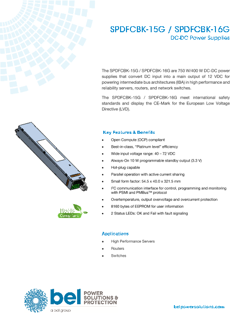
The SPDFCBK-15G / SPDFCBK-16G are 750 W/400 W DC-DC power
supplies that convert DC input into a main output of 12 VDC for
powering intermediate bus architectures (IBA) in high performance and
reliability servers, routers, and network switches.
The SPDFCBK-15G / SPDFCBK-16G meet international safety
standards and display the CE-Mark for the European Low Voltage
Directive (LVD).
Open Compute (OCP) compliant
Best-in-class, “Platinum level” efficiency
Wide input voltage range: 40 – 72 VDC
Always-On 10 W programmable standby output (3.3 V)
Hot-plug capable
Parallel operation with active current sharing
Small form factor: 54.5 x 40.0 x 321.5 mm
I2C communication interface for control, programming and monitoring
with PSMI and PMBus™ protocol
Overtemperature, output overvoltage and overcurrent protection
8160 bytes of EEPROM for user information
2 Status LEDs: OK and Fail with fault signaling
High Performance Servers
Routers
Switches
Page2
2 SPDFCBK-15G / SPDFCBK-16G
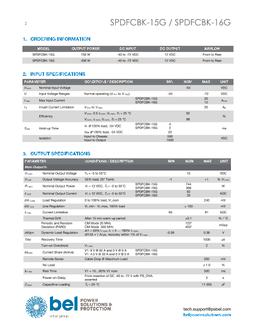
SPDFCBK-15G 750 W -40 to -72 VDC 12 VDC Front to Rear
SPDFCBK-16G 400 W -40 to -72 VDC 12 VDC Front to Rear
Vi nom Nominal Input Voltage -54 VDC
Vi Input Voltage Ranges Normal operating (Vi min to Vi max) -40 -72 VDC
SPDFCBK-15G 25
Ii max Max Input Current Arms
SPDFCBK-16G 12
Ii p Inrush Current Limitation Vi min to Vi max 20 Ap
Vi nom, 0.5∙Ix nom, Vx nom, TA = 25 °C 92
Efficiency %
Vi nom, Ix nom, Vx nom, TA = 25 °C 88
SPDFCBK-15G 4
V1 @ 100% load, -54 VDC
Thold Hold-up Time SPDFCBK-16G 2 ms
VSB @ 100% load, -54 VDC 20
Input to Chassis 500
Isolation VDC
Input to Output 1500
Main Output V1
V1 nom Nominal Output Voltage Ta = -5 to 55°C 12 VDC
V1 set Output Voltage Accuracy 50% load, 25° Tamb -1 +1 % V1 nom
SPDFCBK-15G 744
P1 nom Nominal Output Power V1 = 12 VDC, Ta = -5 to 55°C W
SPDFCBK-16G 396
SPDFCBK-15G 62
I1 nom Nominal Output Current V1 = 12 VDC, Ta = -5 to 55°C ADC
SPDFCBK-16G 33
dV1 Load Load Regulation 0 to 100% load, Vi_nom 240 mV
dV1 Line Line Regulation Vi_min - Vi_max, 100% load ± 100 mV
I1 max Current Limitation 65 81 ADC
Thermal Drift After 15 min warm up period ±0.1 % / °C
Periodic and Random CM Mode 20 MHz 120*
mVpp
Deviation (PARD) CM Mode 500 MHz 400*
ΔI1 = 50% I1 nom, I1 = 5 … 100% I1 nom,
dVdyn Dynamic Load Regulation -0.36 0.36 V
dI1/dt = 1 A/μs, recovery within 1% of V1 nom
Trec Recovery Time 1000 μs
Turn-on Overshoot V1 nom 2 %
V1: 8 V @ 62 A and 0 V @ 0 A SPDFCBK-15G
dIshare Current Share (Active)
V1: 4.3 V @ 33 A and 0 V @ 0 A SPDFCBK-16G
Remote Sense Cable Drop @ Maximum Load 200 mV
No Load ± 1.0 %
tV1 rise Rise Time V1 = 10…90% V1 nom 500 ms
From insertion of DC -40 to -72 V with PS_ON/L
Power-on-Delay 3 s
asserted
CLoad Capacitive Loading Ta = 25 °C 11 000 μF
tech.support@psbel.com
Page3
SPDFCBK-15G / SPDFCBK-16G 3
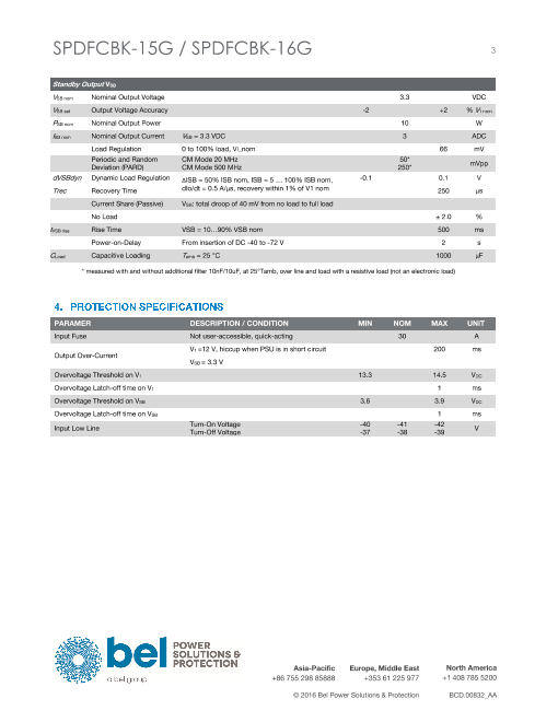
Standby Output VSB
VSB nom Nominal Output Voltage 3.3 VDC
VSB set Output Voltage Accuracy -2 +2 % V1 nom
PSB nom Nominal Output Power 10 W
ISB nom Nominal Output Current VSB = 3.3 VDC 3 ADC
Load Regulation 0 to 100% load, Vi_nom 66 mV
Periodic and Random CM Mode 20 MHz 50*
mVpp
Deviation (PARD) CM Mode 500 MHz 250*
dVSBdyn Dynamic Load Regulation ΔISB = 50% ISB nom, ISB = 5 … 100% ISB nom, -0.1 0.1 V
Trec Recovery Time dIo/dt = 0.5 A/μs, recovery within 1% of V1 nom 250 μs
Current Share (Passive) VSB: total droop of 40 mV from no load to full load
No Load ± 2.0 %
tVSB rise Rise Time VSB = 10…90% VSB nom 500 ms
Power-on-Delay From insertion of DC -40 to -72 V 2 s
CLoad Capacitive Loading Tamb = 25 °C 1000 μF
* measured with and without additional filter 10nF/10uF, at 25°Tamb, over line and load with a resistive load (not an electronic load)
PARAMER DESCRIPTION / CONDITION MIN NOM MAX UNIT
Input Fuse Not user-accessible, quick-acting 30 A
V1 =12 V, hiccup when PSU is in short circuit 200 ms
Output Over-Current
VSB = 3.3 V
Overvoltage Threshold on V1 13.3 14.5 VDC
Overvoltage Latch-off time on V1 1 ms
Overvoltage Threshold on VSB 3.6 3.9 VDC
Overvoltage Latch-off time on VSB 1 ms
Turn-On Voltage -40 -41 -42
Input Low Line V
Turn-Off Voltage -37 -38 -39
Asia-Pacific Europe, Middle East North America
+86 755 298 85888 +353 61 225 977 +1 408 785 5200
© 2016 Bel Power Solutions & Protection BCD.00832_AA
Page4
4 SPDFCBK-15G / SPDFCBK-16G
5.1 Status signals
CONDITION STATUS SIGNALS LEDS
(Assuming 2 or more power supplies present and ON and STBY
shared for management interface)
No problems and power supply is on 1 1 0 0 0 Solid green off
V1 12V Over current 1 0 0 0 0 off Solid amber
DC input fail 0 0 0 0 0 off off
UV on V1 and PS has latched off 1 0 0 0 0 off Solid amber
UV on VSB and the V1 is latched off 1 0 0 0 0 off Solid amber
OV on V1 or VSB and PS has latched off (UV set as output off) 1 0 0 0 0 off Solid amber
Over temperature shutdown and PS has turned off 1 0 0 0 0 off Solid amber
Fan error (>15%) 1 0 0 0 0 off Solid amber
Over temperature warning 1 1 0 0 0 off 1Hz blinking
PSON High (VSB on) 1 0 1 0 0 1Hz blinking off
Fan blocked or running under speed (5-15%) but outputs still within
spec and not over temp. This is a warning condition. off 1Hz blinking
Redundant operation (2 or more power supplies in parallel) – PSU1 1 1 0 0 0
operating; PSU2 has input power removed. Till input power from PSU1 off (PSU2) off (PSU2)
is removed.
5.2 GRAPHICAL USER INTERFACE
The Bel Power Solutions provides with its “I2C Utility” a Windows® XP/Vista/Win7 compatible graphical user interface
allowing the programming and monitoring of the SPDFCBK-15G / SPDFCBK-16G Front-End. The utility can be downloaded
on www.belpowersolutions.com and supports both the PSMI and PMBus™ protocols.
The GUI allows automatic discovery of the units connected to the communication bus and will show them in the navigation
tree. In the monitoring view the power supply can be controlled and monitored.
If the GUI is used in conjunction with the SPDFCBK-15G / SPDFCBK-16G Evaluation Kit it is also possible to control the
PSON pin(s) of the power supply.
Further there is a button to disable the internal fan for approximately 5 seconds (not implemented yet). This allows the user to
take input power measurements without fan consumptions to check efficiency compliance to the Climate Saver Computing
Platinum specification.
tech.support@psbel.com
Input OK/H
PWOK/H
PSON/L
PRESENT/L
PS KILL
PWR OK
FAIL
Page5
SPDFCBK-15G / SPDFCBK-16G 5
The monitoring screen also allows to enable the hot-standby mode on the power supply. The mode status is monitored and
by changing the load current it can be monitored when the power supply is being disabled for further energy savings. This
obviously requires 2 power supplies being operated as a redundant system (like the evaluation kit).
NOTE: The user of the GUI needs to ensure that only one of the power supplies have the hot-standby mode enabled.
Approved to the latest edition of the following standards: UL/CSA60950-1, IEC60950-1 and EN60950-1.
Asia-Pacific Europe, Middle East North America
+86 755 298 85888 +353 61 225 977 +1 408 785 5200
© 2016 Bel Power Solutions & Protection BCD.00832_AA
Page6
6 SPDFCBK-15G / SPDFCBK-16G
7.1 IMMUNITY
IEC / EN 61000-4-2, ±8 kV, 25+25 discharges per test point
ESD Contact Discharge B
(metallic case, LEDs, connector body)
IEC / EN 61000-4-2, ±15 kV, 25+25 discharges per test point
ESD Air Discharge B
(non-metallic user accessible surfaces)
IEC / EN 61000-4-3, 10 V/m, 1 kHz/80% Amplitude Modulation,
Radiated Electromagnetic Field A
1 µs Pulse Modulation, 10 kHz…2 GHz
IEC / EN 61000-4-4, level 3
Electrical Fast Transient / Burst B
Input DC port ±2 kV, 1 minute
IEC / EN 61000-4-5
Surge Line to earth: ±1 kV A
Line to line: ±1 kV
RF Conducted Immunity IEC/EN 61000-4-6, Level 3, 10 Vrms, CW, 0.1 … 80 MHz A
7.2 EMISSION
EN55022 / CISPR 22: Class A
single unit, @ -54 VDC, full load 6 dB margin
Conducted Emission
EN55022 / CISPR 22: Class A
2 units in rack system, @ -54 VDC, full load of single unit 6 dB margin
EN55022 / CISPR 22: Class A
single unit, @ -54 VDC, full load 6 dB margin
Radiated Emission
EN55022 / CISPR 22: Class A
2 units in rack system, @ -54 VDC, full load of single unit 6 dB margin
Operating -5 +55
Temperature °C
Non-Operating -40 +85
Operating 90
Humidity 0 %RH
Non-Operating (non-condescending) 95
up to 40°C 4000
Altitude Operating with no degradation m
up to 55°C 1800
Operating: three half-sine mechanical shocks 30G with pulse
width 16 mm
Shock
Non-operating: half-sine mechanical shocks 30G with pulse
width 16 mm, 18 shocks in three axis in both directions
Operating: Swept Sine 1G peak, 5-500-5Hz
Vibration
Non-operating: Swept Sine 4G peak, 5-500-5Hz
Audible Noise Sound power @Vi nom, 50% load, TA = 27°C 53 dBA
Width 54.5
Dimensions Height 40.0 mm
Depth 321.55
M Weight 0.918 kg
tech.support@psbel.com
Page7
SPDFCBK-15G / SPDFCBK-16G 7
321.55 ±0.5
12.66 ±.020
27.8 20.4
1.09 .80 TYCO P/N 1926736-2
AIRFLOW DIRECTION ∗
Figure 1. Side View 1
BEL POWER AGENCY LABEL
(ALSO INCLUDE WEE, EDUP
AND PB-FREE / ROHS LOGO)
19.93
.78
HANDLE
4.3
.17
7.16
.28
329.28 ±0.5
12.96 ±.020
333.55 ±0.5
13.13 ±.020
Figure 2. Top View
54.5 ±0.5
2.15 ±.020
9 ±0.5
PIN A1
.35 ±.020
Figure 3. Front View Figure 4. Rear View
10.1 INPUT CONNECTOR
Unit: PHOENIX CONTACT, PC 5/2-GF-7,62
Counter part: PHOENIX CONTACT, PC 5/2-STF-7.62 BD
1 V_RTN Input voltage (positive)
2 V_IN Input power ground (return)
Asia-Pacific Europe, Middle East North America
+86 755 298 85888 +353 61 225 977 +1 408 785 5200
© 2016 Bel Power Solutions & Protection BCD.00832_AA
8.3
.33
40 ±0.5
1.57 ±.020 12.5.49
3
.118
3.6 ±0.5
.14 ±.020
Page8
8 SPDFCBK-15G / SPDFCBK-16G
10.2 OUTPUT CONNECTOR
Unit: Tyco Electronics P/N 2-1926736-2 NOTE: Column 5 is lagging (short pins)
Counter part: Tyco Electronics P/N 2-1926733-5
PIN SIGNAL NAME DESCRIPTION AMPS PER PIN
1 PGND Power ground (return) 25
2 PGND Power ground (return) 25
3 PGND Power ground (return) 25
4 PGND Power ground (return) 25
5 PGND Power ground (return) 25
6 V1 +12 VDC main output 25
7 V1 +12 VDC main output 25
8 V1 +12 VDC main output 25
9 V1 +12 VDC main output 25
10 V1 +12 VDC main output 25
A1 VSB Standby positive output (+3.3V)
B1 VSB Standby positive output (+3.3V)
C1 VSB Standby positive output (+3.3V)
D1 VSB Standby positive output (+3.3V)
E1 VSB Standby positive output (+3.3V)
A2 SGND Signal ground (return)
B2 SGND Signal ground (return)
C2 nc No connect
D2 nc No connect
E2 nc No connect
A3 PSKILL Power supply kill (lagging pin)
B3 nc No connect
C3 SDA I2C data signal line
D3 V1_SENSE_R Main output negative sense
E3 V1_SENSE Main output positive sense
A4 SCL I2C clock signal line
B4 PSON PS on input connect (referenced to A2/B2)
C4 SMB_ALERT SMB Alert signal output
D4 ISHARE Current share signal
E4 INPUT_OK DC input OK signal
A5 A0 Address 0
B5 nc No connect
C5 PWOK Power OK signal output
D5 A1 Address 1
E5 PRESENT_L Power supply present
Table 2. Pin Description
tech.support@psbel.com
Page9
SPDFCBK-15G / SPDFCBK-16G 9
I2C Utility
Windows XP/Vista/7 compatible GUI to belpowersolutions.com
N/A
program, control and monitor Front-Ends
(and other I2C units)
USB to I2C Converter
Master I2C device to program, control and
2 2 ZM-00056 Bel Power Solutions monitor I C units in conjunction with the I C
Utility
Dual Connector Board
Connector board to operate 2 units in
SNP-OP-BOARD-01 Bel Power Solutions
parallel. Includes an on-board USB to I2C
converter (use I2C Utility as desktop software)
NUCLEAR AND MEDICAL APPLICATIONS - Products are not designed or intended for use as critical components in life support
systems, equipment used in hazardous environments, or nuclear control systems.
TECHNICAL REVISIONS - The appearance of products, including safety agency certifications pictured on labels, may change
depending on the date manufactured. Specifications are subject to change without notice.
Asia-Pacific Europe, Middle East North America
+86 755 298 85888 +353 61 225 977 +1 408 785 5200
© 2016 Bel Power Solutions & Protection BCD.00832_AA