


Non-Isolated, Fixed Ratio DC-DC Converter
このカタログについて
| ドキュメント名 | NBM Bus Converter NBM2317S60E1560T0R |
|---|---|
| ドキュメント種別 | 製品カタログ |
| ファイルサイズ | 2.7Mb |
| 取り扱い企業 | Vicor株式会社 (この企業の取り扱いカタログ一覧) |
この企業の関連カタログ


このカタログの内容
Page1
NBM™ Bus Converter
NBM2317S60E1560T0R
Non-Isolated, Fixed Ratio DC-DC Converter
Features & Benefits
Product Ratings (Step-Down Operation)
• Maximum continuous output power: 800W
VHI = 54V (38 – 60V) ILO = up to 60A
Up to 1kW, 2ms peak power capability
V = 13.5V (9.5 – 15V)
• Rated output current (step-down operation): LO K = 1/4(no load)
60A continuous
100A transient, up to 2ms Product Description
• Rated output current (step-up operation):
The NBM2317S60E1560T0R is a high-efficiency Non-Isolated Bus
15A continuous Converter operating from a 38 to 60VDC high-side voltage bus to
25A transient, up to 2ms deliver a ratiometric low-side voltage from 9.5 to 15VDC.
• Up to 4.5kW/in3 power density The NBM2317S60E1560T0R offers low noise, fast transient
response, and industry-leading efficiency and power density. In
• 97.9% peak efficiency addition, it provides an AC impedance beyond the bandwidth of
• Parallel operation for multi-kW arrays most downstream regulators, allowing input capacitance normally
located at the input of a PoL regulator to be located at the high
• OV, OC, UV, short circuit and thermal protection side of the NBM. With a high-side to low-side K factor of 1/4, that
• NBM2317 SM-ChiP™ package capacitance value can be reduced by a factor of 16x, resulting in
savings of board area, material and total system cost.
0.899 x 0.683 x 0.292in
[22.83 x 17.34 x 7.42mm] Leveraging the thermal and density benefits of Vicor SM-ChiP
packaging technology, the NBM offers flexible thermal
• Thermally-adept SM-ChiP management options with very low top- and bottom-side thermal
impedances. Thermally-adept SM-ChiP-based power components
• Bidirectional start up and steady-state operation enable customers to achieve low-cost power system solutions
• Simple implementation, no external components required with previously unattainable system size, weight and efficiency
attributes quickly and predictably.
• Built-in hot-swap capabilities and inrush current limiting
The NBM non-isolated topology allows bidirectional start up and
steady-state operation and provides bidirectional protections.
Typical Applications
• DC Power Distribution
• High-Performance Computing Systems (HPC)
• Mild Hybrid and Autonomous Vehicles
• Automated Test Equipment (ATE)
• Industrial Systems
• High-Density Power Supplies
• Communications Systems
• Transportation
• Bidirectional DC Energy Storage
Note: Product images may not highlight current product markings.
NBM™ Bus Converter Rev 1.4
Page 1 of 31 11/2019
Page2
NBM2317S60E1560T0R
Typical Applications
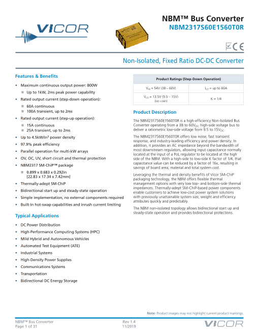
NBM
TM / OG
EN
enable/disable
switch
FUSE
+VHI +VLO
PGND
V PGNDHI
HI SIDE LO SIDE
CI_NBM_ELEC PoL
SOURCE_RTN
NBM2317S60E1560T0R + point-of-load
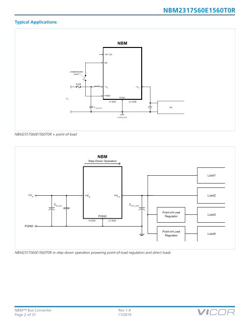
NBM
Step-Down Operation
Load1
+VHI +VHI +VLO Load2
CIN_EXT COUT_EXT
Point-of-Load
PGND Regulator Load3
HI SIDE LO SIDE
PGND
Point-of-Load
Regulator Load4
NBM2317S60E1560T0R in step-down operation powering point-of-load regulators and direct loads
NBM™ Bus Converter Rev 1.4
Page 2 of 31 11/2019
Page3
NBM2317S60E1560T0R
Typical Applications (Cont.)
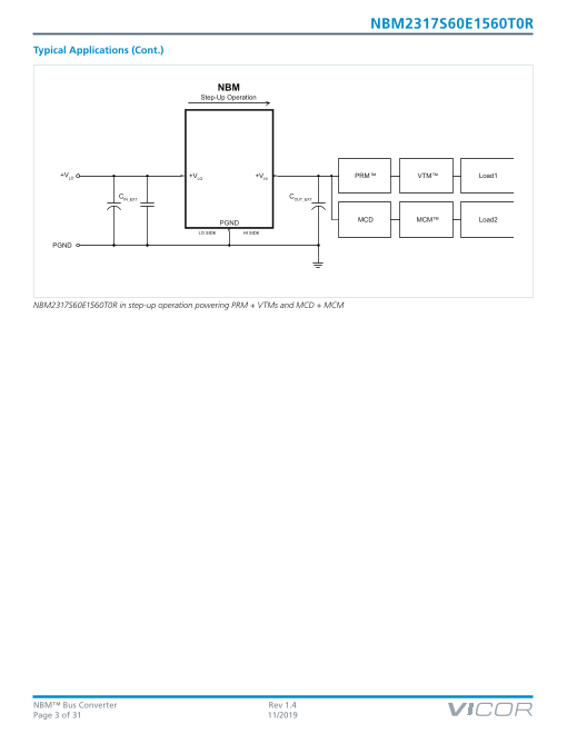
NBM
Step-Up Operation
+VLO +VLO +VHI PRM™ VTM™ Load1
CIN_EXT COUT_EXT
PGND MCD MCM™ Load2
LO SIDE HI SIDE
PGND
NBM2317S60E1560T0R in step-up operation powering PRM + VTMs and MCD + MCM
NBM™ Bus Converter Rev 1.4
Page 3 of 31 11/2019
Page4
NBM2317S60E1560T0R
Pin Configuration
TOP VIEW
+VHI 1
TM / OG 2 6 5 +V
PGND LOEN 3
+VHI 4
NBM2317 SM-ChiP™
Top-side indicator
Pin Descriptions
Pin Number Signal Name Type Function
1, 4 +VHI HIGH SIDE POWER High-side power positive terminals
2 TM / OG OUTPUT Temperature Monitor and Output Good
3 EN INPUT Enables / disables NBM. When held low, the unit will be disabled
5 +VLO LOW SIDE POWER Low-side power positive terminal
6 PGND POWER RETURN Common negative high-side and low-side power return terminal
NBM™ Bus Converter Rev 1.4
Page 4 of 31 11/2019
Page5
NBM2317S60E1560T0R
Part Ordering Information
Part Number Temperature Grade Option Tray Size
NBM2317S60E1560T0R T = –40 to 125°C 0R = Reversible Analog Control 55 parts per tray
All products shipped in JEDEC standard high-profile (0.400” thick) trays (JEDEC Publication 95, Design Guide 4.10).
Absolute Maximum Ratings
The absolute maximum ratings below are stress ratings only. Operation at or beyond these maximum ratings can cause permanent damage to the device.
Parameter Comments Min Max Unit
+VHI_DC to PGND –1 80 V
VHI_DC or VLO_DC Slew Rate
1 V/µs
(Operational)
+VLO_DC to PGND –1 16.9 V
TM to PGND 7 V
–0.3
EN to PGND 15 V
NBM™ Bus Converter Rev 1.4
Page 5 of 31 11/2019
Page6
NBM2317S60E1560T0R
Electrical Specifications
Specifications apply over all line and load conditions, unless otherwise noted; boldface specifications apply over the temperature range of
–40°C ≤ TINTERNAL ≤ 125°C (T-Grade); all other specifications are at TINTERNAL = 25ºC unless otherwise noted.
Attribute Symbol Conditions / Notes Min Typ Max Unit
General Powertrain Specification – Step-Down Operation (High-Voltage Side to Low-Voltage Side)
High-Side Input Voltage Range
VHI_DC 38 60 V(Continuous)
Disabled, EN low, VHI_DC = 54V 1.5
High-Side Input Quiescent Current IHI_Q mA
TINTERNAL ≤ 100ºC 3.0
VHI_DC = 54V, TINTERNAL = 25ºC 3.6 7
VHI_DC = 54V 2 11
No Load Power Dissipation PHI_NL W
VHI_DC = 38 – 60V, TINTERNAL = 25ºC 8
VHI_DC = 38 – 60V 14.5
VHI_DC = 54V, CLO_EXT = 1000μF, no load 7.5
High-Side Input Inrush Current Peak IHI_INR_PK A
TINTERNAL ≤ 100ºC 12
DC High-Side Input Current IHI_IN_DC At ILO_OUT_DC = 60A, TINTERNAL ≤ 100ºC 16.3 A
High voltage side to low voltage side,
Transformation Ratio K 1/4 V/V
K = VLO_DC / VHI_DC, at no load
Low-Side Output Current
ILO_OUT_DC 38V ≤ VHI_DC ≤ 60V 60 A(Continuous)
2ms pulse, 25% duty cycle,
Low-Side Output Current (Pulsed) ILO_OUT_PULSE 100 AILO_OUT_AVG ≤ 50% rated ILO_OUT_DC
Low-Side Output Power (Continuous) PLO_OUT_DC 54V < VHI_DC ≤ 60V 800 W
2ms pulse, 25% duty cycle,
Low-Side Output Power (Pulsed) PLO_OUT_PULSE 1000 WPLO_OUT_AVG ≤ 50% rated PLO_OUT_DC
VHI_DC = 54V, ILO_OUT_DC = 60A 97.0 97.4
Efficiency (Ambient) η V = 38 – 60V, I = 60A 96.2 %
AMB HI_DC LO_OUT_DC
VHI_DC = 54V, ILO_OUT_DC = 30A 97.3 97.8
VHI_DC = 54V, ILO_OUT_DC = 60A 96.7 97.4
Efficiency (Hot) η %
HOT VHI_DC = 54V, ILO_OUT_DC = 30A 97.3 97.9
Efficiency (Over Load Range) η 12A < I < 60A 92.0 %
20% LO_OUT_DC
RLO_COLD VHI_DC = 54V, ILO_OUT_DC = 60A, TINTERNAL = –40°C 2.6 3.3 4
Low-Side Output Resistance RLO_AMB VHI_DC = 54V, ILO_OUT_DC = 60A 3.5 4.4 5.3 mΩ
RLO_HOT VHI_DC = 54V, ILO_OUT_DC = 60A, TINTERNAL = 100°C 4.4 5.5 5.7
Switching Frequency FSW Low-side voltage ripple frequency = 2x FSW 1.57 1.62 1.67 MHz
CLO_EXT = 0μF, ILO_OUT_DC = 60A, VHI_DC = 54V, 120
Low-Side Output Voltage Ripple V 20MHz BWLO_OUT_PP mV
TINTERNAL ≤ 100ºC 180
Effective High-Side Input
C Effective value at 54V 11.2 µF
Capacitance (Internal) HI_INT HI_DC
Effective Low-Side Output
C Effective value at 13.5V 55 µF
Capacitance (Internal) LO_INT LO_DC
Rated Low-Side Output Excessive capacitance may drive module
C 1000 µF
Capacitance (External) LO_OUT_EXT into short circuit protection
Rated Low-Side Output Capacitance CLO_OUT_AEXT Max = N • 0.5 • CLO_OUT_EXT MAX, C 500 µF
(External), Parallel Array Operation LO_OUT_AEXT where N = the number of units in parallel
NBM™ Bus Converter Rev 1.4
Page 6 of 31 11/2019
Page7
NBM2317S60E1560T0R
Electrical Specifications (Cont.)
Specifications apply over all line and load conditions, unless otherwise noted; boldface specifications apply over the temperature range of
–40°C ≤ TINTERNAL ≤ 125°C (T-Grade); all other specifications are at TINTERNAL = 25ºC unless otherwise noted.
Attribute Symbol Conditions / Notes Min Typ Max Unit
Powertrain Protection Specification – Step-Down Operation (High-Voltage Side to Low-Voltage Side), Cont.
Start up into a persistent fault condition. Non-latching
Auto Restart Time tAUTO_RESTART 350 500 600 msfault detection given VHI_DC > VHI_UVLO+
High-Side Input Overvoltage
VHI_OVLO+ 64.6 66 VLockout Threshold
High-Side Input Overvoltage
VHI_OVLO– 60 64 VRecovery Threshold
High-Side Input Overvoltage
V 0.4 V
Lockout Hysteresis HI_OVLO_HYST
High-Side Input Overvoltage
t 1 µs
Lockout Response Time HI_OVLO
High-Side Input Undervoltage
VHI_UVLO– 31.6 33.2 VLockout Threshold
High-Side Input Undervoltage
V
Recovery Threshold HI_UVLO+
35 38 V
High-Side Input Undervoltage
V 2 V
Lockout Hysteresis HI_UVLO_HYST
High-Side Input Undervoltage
t 100 µs
Lockout Response Time HI_UVLO
From V = V to powertrain active,
Input-to-Output Undervoltage HI_DC HI_UVLO+
t
Start-Up Delay HI_TO_LO_DELAY
EN floating (i.e., one-time start-up delay from 600 ms
application of VHI_DC to VLO_DC)
Low-Side Output Soft-Start From powertrain active; fast current limit protection
t
Ramp Time LO_SOFT_START
0.5 ms
disabled during soft start
Low-Side Output Overcurrent
I
Trip Threshold LO_OUT_OCP
61 75 110 A
Low-Side Output Overcurrent
t
Response Time Constant LO_OUT_OCP
Effective internal RC filter 2 5 ms
Low-Side Output Short Circuit
I
Protection Trip Threshold LO_OUT_SCP
100 A
Low-Side Output Short Circuit
t 1 µs
Protection Response Time LO_OUT_SCP
Overtemperature
tOTP+ Temperature sensor located inside controller IC 125 °CShutdown Threshold
Overtemperature
t 105 110 115 °C
Recovery Threshold OTP–
Undertemperature
t Temperature sensor located inside controller IC –45 °C
Shutdown Threshold UTP
NBM™ Bus Converter Rev 1.4
Page 7 of 31 11/2019
Page8
NBM2317S60E1560T0R
Electrical Specifications (Cont.)
Specifications apply over all line and load conditions, unless otherwise noted; boldface specifications apply over the temperature range of
–40°C ≤ TINTERNAL ≤ 125°C (T-Grade); all other specifications are at TINTERNAL = 25ºC unless otherwise noted.
Attribute Symbol Conditions / Notes Min Typ Max Unit
General Powertrain Specification – Step-Up Operation (Low-Voltage Side to High-Voltage Side)
Low-Side Input Voltage Range
(Start Up) 10.8 15
VLO_DC V
Low-Side Input Voltage Range
(Continuous) 9.5 15
Disabled, EN low, VLO_DC = 13.5V 0.6
Low-Side Input Quiescent Current ILO_Q mA
TINTERNAL ≤ 100ºC 1.2
VLO_DC = 13.5V, TINTERNAL = 25ºC 4.3 7
VLO_DC = 13.5V 3 11
No Load Power Dissipation PLO_NL W
VLO_DC = 9.5 – 15V, TINTERNAL = 25 ºC 8
VLO_DC = 9.5 – 15V 14
VLO_DC = 15V, CHI_EXT = 68μF, no load 45
Low-Side Input Inrush Current Peak ILO_INR_PK A
TINTERNAL ≤ 100ºC 60
DC Low-Side Input Current ILO_IN_DC At IHI_OUT_DC = 15A, TINTERNAL ≤ 100ºC 62 A
Low-voltage side to high-voltage side,
Transformation Ratio K 4 V/V
K = VHI_DC / VLO_DC, at no load
High-Side Output Current
IHI_OUT_DC 9.5V ≤ VLO_DC ≤ 13.5V 15 A(Continuous)
2ms pulse, 25% duty cycle,
High-Side Output Current (Pulsed) IHI_OUT_PULSE 25 AIHI_OUT_AVG ≤ 50% rated IHI_OUT_DC
High-Side Output Power
P
(Continuous) HI_OUT_DC
13.5V < VLO_DC ≤ 15V 800 W
2ms pulse, 25% duty cycle,
High-Side Output Power (Pulsed) PHI_OUT_PULSE 1000 WPHI_OUT_AVG ≤ 50% rated PHI_OUT_DC
VLO_DC = 13.5V, IHI_OUT_DC = 15A 96.9 97.3
Efficiency (Ambient) η VLO_DC = 9.5 – 15V, IHI_OUT_DC = 15A 96.2 %AMB
VLO_DC = 13.5V, IHI_OUT_DC = 7.5A 97.3 97.9
VLO_DC = 13.5V, IHI_OUT_DC = 15A 96.7 97.0
Efficiency (Hot) η %
HOT VLO_DC = 13.5V, IHI_OUT_DC = 7.5A 97.3 97.8
Efficiency (Over Load Range) η 3A < I < 15A 92.0 %
20% HI_OUT_DC
RHI_COLD VLO_DC = 13.5V, IHI_OUT_DC = 15A, TINTERNAL = –40°C 50 65 80
High-Side Output Resistance RHI_AMB VLO_DC = 13.5V, IHI_OUT_DC = 15A 62 80 98 mΩ
RHI_HOT VLO_DC = 13.5V, IHI_OUT_DC = 15A, TINTERNAL = 100°C 75 97 118
Switching Frequency FSW High-side output voltage ripple frequency = 2x FSW 1.57 1.62 1.67 MHz
CHI_EXT = 0μF, IHI_OUT_DC = 15A, VLO_DC = 13.5V, 138
High-Side Output Voltage Ripple V 20MHz BWHI_OUT_PP mV
TINTERNAL ≤ 100ºC 200
Effective Low-Side Input Capacitance
C Effective value at 13.5V
(Internal) LO_INT LO_DC
55 µF
Effective High-Side
CHI_INT Effective value at 54V 11.2 µFOutput Capacitance (Internal) HI_DC
Rated High-Side Output Capacitance At start up with no load; excessive capacitance may
C µF
(External) HI_OUT_EXT prevent module start up 68
Rated High-Side Output Capacitance C
C HI_OUT_AEXT
Max = N • 0.5 • CHI_OUT_EXT MAX,
(External), Parallel Array Operation HI_OUT_AEXT
34 µF
where N = the number of units in parallel
NBM™ Bus Converter Rev 1.4
Page 8 of 31 11/2019
Page9
NBM2317S60E1560T0R
Electrical Specifications (Cont.)
Specifications apply over all line and load conditions, unless otherwise noted; boldface specifications apply over the temperature range of
–40°C ≤ TINTERNAL ≤ 125°C (T-Grade); all other specifications are at TINTERNAL = 25ºC unless otherwise noted.
Attribute Symbol Conditions / Notes Min Typ Max Unit
Powertrain Protection Specification – Step-Up Operation (Low-Voltage Side to High-Voltage Side), Cont.
Start up into a persistent fault condition. Non-latching
Auto Restart Time tAUTO_RESTART 350 500 600 msfault detection given VLO_DC > VLO_UVLO+
Low-Side Input Overvoltage
V 16.7 V
Lockout Threshold LO_OVLO+ 17.2
Low-Side Input Overvoltage
V
Recovery Threshold LO_OVLO– 15.4
15.8 V
Low-Side Input Overvoltage
V
Lockout Hysteresis LO_OVLO_HYST
0.1 V
Low-Side Input Overvoltage
t 1 µs
Lockout Response Time LO_OVLO
Low-Side Input Undervoltage
V 8.6 V
Lockout Threshold LO_UVLO– 8.0
Low-Side Input Undervoltage
V
Recovery Threshold LO_UVLO+
10.5 10.8 V
Low-Side Input Undervoltage
V
Lockout Hysteresis LO_UVLO_HYST
0.1 V
Low-Side Input Undervoltage
t 8 µs
Lockout Response Time LO_UVLO
From V
Input-to-Output LO_DC
= VLO_UVLO+ to powertrain active,
tLO_TO_HI_DELAY EN floating (i.e., one-time start-up delay from 600 msStart-Up Delay
application of VLO_DC to VHI_DC)
High-Side Output
tHI_SOFT_START From powertrain active. 500 µsSoft-Start Ramp Time
Protection will stop powertrain; conduction path from
High-Side Output Overcurrent
IHI_OUT_OCP low side to high side still exists through body diodes of 18.75 ATrip Threshold 15.25 27.5
powertrain MOSFETs [a]
High-Side Output Overcurrent
t Effective internal RC filter 2 5 ms
Response Time Constant HI_OUT_OCP
Overtemperature
t Temperature sensor located inside controller IC
Shutdown Threshold OTP+ 125
°C
Overtemperature
t 105 110 115 °C
Recovery Threshold OTP–
Undertemperature
tUTP Temperature sensor located inside controller IC –45 °CShutdown Threshold
[a] Sustained current through body diodes can cause powertrain damage. See "start up and bidirectional operation" on page 21.
NBM™ Bus Converter Rev 1.4
Page 9 of 31 11/2019
Page10
NBM2317S60E1560T0R
Operating Area
70 Isothermal Surfaces
60
Top
50
Top-side
40 indicator
30
20 Bottom
10
0
40 50 60 70 80 90 100 110 120 130
Leads
Temperature (ºC)
Top Only Bottom with Leads
Top, Bottom, with Leads Note: Generic SM-ChiP™ package shown. Representation may not
match specific footprint of the product in this data sheet.
Figure 1 — Specified thermal operating area
1100 110
1000 100
900 90
800 80
700 70
600 60
500 50
400 40
300 30
200 20
100 10
0 0
38 40 42 44 46 48 50 52 54 56 58 60 38 40 42 44 46 48 50 52 54 56 58 60
High-Side Input Voltage ( V) High-Side Input Voltage ( V)
PLO_OUT_DC PLO_OUT_PULSE ILO_OUT_DC ILO_OUT_PULSE
Figure 2 — Specified electrical operating area, step-down operation
1100 30
1000
900 25
800
700 20
600
500 15
400 10
300
200 5
100
0 0
9.5 10.0 10.5 11.0 11.5 12.0 12.5 13.0 13.5 14.0 14.5 15.0 9.5 10.0 10.5 11.0 11.5 12.0 12.5 13.0 13.5 14.0 14.5 15.0
Low-Side Input Voltage ( V) Low-Side Input Voltage ( V)
P IHI_OUT_DC PHI_OUT_PULSE HI_OUT_DC IHI_OUT_PULSE
Figure 3 — Specified electrical operating area, step-up operation
NBM™ Bus Converter Rev 1.4
Page 10 of 31 11/2019
High-Side Output Powe r (W) Low-Side Output Powe r (W)
Output Current (A)
High-Side Output Current (A) Low-Side Output Curre nt (A)
Page11
NBM2317S60E1560T0R
Signal Characteristics
Specifications apply over all line and load conditions, unless otherwise noted; boldface specifications apply over the temperature range of
–40°C ≤ TINTERNAL ≤ 125°C (T-Grade); all other specifications are at TINTERNAL = 25ºC unless otherwise noted.
Temperature Monitor / Output Good (TM / OG)
• The TM/OG pin provides temperature monitoring and power good functionalities.
• The TM/OG is internally held low (0V) until the start up has completed.
• This signal can be used to drive logic circuit downstream for delayed enable of the load.
• After start up, this pin provides a voltage proportional to the absolute temperature of the converter control IC.
• For more information, see signal pin description section, page 21.
Signal Type State Attribute Symbol Conditions / Notes Min Typ Max Unit
Powertrain active to
Start Up tTM/OG Powertrain active to TM / OG high µsTM / OG time 1800
TM / OG Voltage Range VTM/OG 2.12 4.04 V
TM / OG
V
Voltage Reference TM/OG_AMB
TJ controller = 27°C 2.95 3.00 3.05 V
Analog
Output Regular TM / OG Source Current ITM/OG TM accuracy = ±5°C 10 µA
Operation TM / OG Short Circuit Maximum source current
I
Current SC_TM/OG
mA
when pulled to ground externally 5
TM / OG Gain ATM/OG 10 mV / °C
TM / OG Voltage Ripple VTM/OG_PP CTM/OG = 0pF, VHI_DC = 54V, ILO_OUT_DC = 60A 120 200 mV
TM / OG Capacitance
C
(External) TM/OG_EXT 50
pF
Transition
Digital TM / OG Fault T
Response Time FR_TM/OG
From fault to TM / OG low 10 µs
Input /
Output TM / OG Voltage VTM/OG_DIS TM/OG held low by internal FET 0 V
Standby Maximum current TM/OG can sink when
TM / OG Sinking Current ISINK_TM/OG mApulled low by internal FET 180
Enable / Disable Control (EN)
• The EN pin enables and disables the NBM. When held low, the NBM is disabled.
• In an array of NBM modules, EN pins should be interconnected to synchronize start up.
• Unit must not be disabled if a load is present on +VHI while operating in step-up mode.
• EN pin outputs 5V during normal operation.
• For more information, see signal pin description, see signal pin description section, page 21.
Signal Type State Attribute Symbol Conditions / Notes Min Typ Max Unit
Regular EN Voltage VEN 4.7 5.0 5.3 V
Operation EN Available Current IEN_OP 2.0 3.5 5.0 mA
Analog EN Source (Current) IEN_EN 50 100 µA
Standby
Output EN Resistance (Internal) REN_INT Internal pull-down resistor 50 150 400 kΩ
Transition EN Capacitance (Internal) CEN_INT 1000 pF
Start Up EN Load Resistance REN_S To permit regular operation 60 kΩ
Regular EN Enable Threshold VEN_EN_TH 2.0 2.5 3.0 V
Operation EN Disable Threshold VEN_DIS_TH 1.95 V
Standby EN Disable Duration tEN_DIS_t Minimum time before attempting re-enable 1 s
Digital EN Threshold Hysteresis VEN_HYSTER 50 mV
Input /
Output EN Enable to Powertrain VHI_DC > VHI_UVLO+, EN held low. Both t µs
Active Time EN_START conditions satisfied for time > t 5 10 30HI_TO_LO_DELAY
Transition
EN Disable to
t µs
VOUT Time
EN_DIS 4 10
EN Fault Response Time tFR_EN From fault to EN low 100 µs
NBM™ Bus Converter Rev 1.4
Page 11 of 31 11/2019
Page12
NBM2317S60E1560T0R
NBM Step-Down Operation Timing Diagram
NBM™ Bus Converter Rev 1.4
Page 12 of 31 11/2019
1 2 3 4 5 6
VHI_OVLO+
VHI_OVLO–
V NLHI
VHI_UVLO+
VHI_UVLO–
EN
5V
3V
C
5V
3V
2.5V
500ms C
before retrial
B
VLO
G
D
LL • K
A E F
ILO
ILO_OUT_SCP
ILO_OUT_OCP
H
TM / OG I I I
3V @ 27°C
0.4V
A: tHI_UVLO+_DELAY E: tEN_START 1: Controller start 4: EN pulled low Notes:
B: tHI_OVLO* F: tLO_OUT_OCP 2: Controller turn o 5: EN released on low-side SC – Timing and signal amplitudes are not to scale
C: tAUTO_RESTART G: tEN_DIS 3: EN release 6: Low-side SC removed – Error pulse width is load dependent
D: tUVLO H: tLO_OUT_SCP**
I: tTM/OG
* Min value switching o
** From detection to powertrain shut down
Page13
NBM2317S60E1560T0R
NBM Step-Up Operation Timing Diagram
NBM™ Bus Converter Rev 1.4
Page 13 of 31 11/2019
1 2 3 4 5
VLO_OVLO+
VLO_OVLO–
V NLLO
VLO_UVLO+
VLO_UVLO–
EN
5V
3V
C
5V
3V
2.5V
500ms C
before retrial
B
VHI
G
D
LL • K
A E F
IHI
IHI_OUT_OCP
TM / OG I I H
3V @ 27°C
0.4V
A: tLO_UVLO+_DELAY E: tEN_START 1: Controller start 4: EN pulled low Notes:
B: tLO_OVLO* F: tHI_OUT_OCP 2: Controller turn o 5: Thermal fault removed – Timing and signal amplitudes are not to scale
C: tAUTO_RESTART G: tEN_DIS 3: EN release – Error pulse width is load dependent
D: tUVLO H: tTM/OG – Blue line: A conduction path from low side to high side
exists through body diodes of powertrain MOSFET.
* Min value switching o When the powertrain is disabled and VLO present,
a voltage equal to VLO minus the body diode
drops will appear on the HI side.
Page14
NBM2317S60E1560T0R
Application Characteristics, Step-Down Operation
Temperature controlled via top side cold plate, unless otherwise noted. All data presented in this section are collected from units operating in step-down
mode, processing power from high-voltage side to low-voltage side. See associated figures for general trend data.
12 6
11
10 5.5
9 5
8
7 4.5
6
5 4
4 3.5
3
2 3
38 40 42 44 46 48 50 52 54 56 58 60 38 40 42 44 46 48 50 52 54 56 58 60
Input Voltage (V) Input Voltage (V)
TCASE: –40ºC 25ºC 85ºC TCASE: –40ºC 25ºC 85ºC
Figure 4 — No-load power dissipation vs. VHI_DC Figure 5 — RLO vs. RHI_IN, ILO_DC = 60A
99 30
98
97 25
96
95 20
94
15
93
92 10
91
90 5
89
88 0
0 6 12 18 24 30 36 42 48 54 60 0 6 12 18 24 30 36 42 48 54 60
Output Current (A) Output Current (A)
VIN: 38V 54V 60V VIN: 38V 54V 60V
Figure 6 — Efficiency at TCASE = –40°C Figure 7 — Power dissipation at TCASE = –40°C
99 30
98.5
98 25
97.5
97 20
96.5
96 15
95.5
95 10
94.5
94 5
93.5
93 0
0 6 12 18 24 30 36 42 48 54 60 0 6 12 18 24 30 36 42 48 54 60
Output Current (A) Output Current (A)
VIN: 38V 54V 60V VIN: 38V 54V 60V
Figure 8 — Efficiency at TCASE = 25°C Figure 9 — Power dissipation at TCASE = 25°C
NBM™ Bus Converter Rev 1.4
Page 14 of 31 11/2019
Efficiency (%) Efficiency (%) No-Load Power Dissipation (W)
Power Dissipation (W) Power Dissipation (W) Output Resistance (mΩ)
Page15
NBM2317S60E1560T0R
Application Characteristics, Step-Down Operation (Cont.)
Temperature controlled via top side cold plate, unless otherwise noted. All data presented in this section are collected from units operating in step-down
mode, processing power from high-voltage side to low-voltage side. See associated figures for general trend data.
99 30
98.5
98 25
97.5
97 20
96.5
96 15
95.5
95 10
94.5
94 5
93.5
93 0
0 6 12 18 24 30 36 42 48 54 60 0 6 12 18 24 30 36 42 48 54 60
Output Current (A) Output Current (A)
VIN: 38V 54V 60V VIN: 38V 54V 60V
Figure 10 — Efficiency at TCASE = 85°C Figure 11 — Power dissipation at TCASE = 85°C
150
125
100
75
50
25
0
0 6 12 18 24 30 36 42 48 54 60
Output Current (A)
VIN: 54V
Figure 12 — VLO_OUT_PP vs. ILO_DC ; no external CLO_OUT_EXT. Figure 13 — Full-load low-side voltage ripple, 68µF CHI_IN_EXT;
Board-mounted module, scope setting: no external CLO_OUT_EXT. Board-mounted module,
20MHz analog BW scope setting: 20MHz analog BW
Figure 14 — 0 – 60A transient response: Figure 15 — 60 – 0A transient response:
CHI_IN_EXT = 68µF, no external CLO_OUT_EXT CHI_IN_EXT = 68µF, no external CLO_OUT_EXT
NBM™ Bus Converter Rev 1.4
Page 15 of 31 11/2019
Output Voltage Ripple (mV ) Efficiency (%)P-P
Power Dissipation (W)
Page16
NBM2317S60E1560T0R
Application Characteristics, Step-Down Operation (Cont.)
Temperature controlled via top side cold plate, unless otherwise noted. All data presented in this section are collected from units operating in step-down
mode, processing power from high-voltage side to low-voltage side. See associated figures for general trend data.
Figure 16 — Start up from application of VHI_DC = 54V, Figure 17 — Start up from application of EN with pre-applied
CLO_OUT_EXT = 1000µF, no load VHI_DC = 54V, CLO_OUT_EXT = 1000µF, no load
NBM™ Bus Converter Rev 1.4
Page 16 of 31 11/2019
Page17
NBM2317S60E1560T0R
Application Characteristics, Step-Up Operation
Temperature controlled via top-side cold plate, unless otherwise noted. All data presented in this section are collected from units operating in step-up mode,
processing power from low-volage side to high-voltage side. See associated figures for general trend data.
12 110
11
10 100
9 90
8
7 80
6
5 70
4 60
3
2 50
9.5 10 10.5 11 11.5 12 12.5 13 13.5 14 14.5 15 9.5 10 10.5 11 11.5 12 12.5 13 13.5 14 14.5 15
Input Voltage (V) Input Voltage (V)
TCASE: –40ºC 25ºC 85ºC TCASE: –40ºC 25ºC 85ºC
Figure 18 — No-load power dissipation vs. VLO_DC Figure 19 — RHI vs. RLO_IN, IHI_DC = 15A
99 30
98
97 25
96
95 20
94
15
93
92 10
91
90 5
89
88 0
0 1.5 3 4.5 6 7.5 9 10.5 12 13.5 15 0 1.5 3 4.5 6 7.5 9 10.5 12 13.5 15
Output Current (A) Output Current (A)
VIN: 9.5V 13.5V 15V VIN: 9.5V 13.5V 15V
Figure 20 — Efficiency at TCASE = –40°C Figure 21 — Power dissipation at TCASE = –40°C
99 30
98.5
98 25
97.5
97 20
96.5
96 15
95.5
95 10
94.5
94 5
93.5
93 0
0 1.5 3 4.5 6 7.5 9 10.5 12 13.5 15 0 1.5 3 4.5 6 7.5 9 10.5 12 13.5 15
Output Current (A) Output Current (A)
VIN: 9.5V 13.5V 15V VIN: 9.5V 13.5V 15V
Figure 22 — Efficiency at TCASE = 25°C Figure 23 — Power dissipation at TCASE = 25°C
NBM™ Bus Converter Rev 1.4
Page 17 of 31 11/2019
Efficiency (%) Efficiency (%) No-Load Power Dissipation (W)
Power Dissipation (W) Power Dissipation (W) Output Resistance (mΩ)
Page18
NBM2317S60E1560T0R
Application Characteristics, Step-Up Operation (Cont.)
Temperature controlled via top-side cold plate, unless otherwise noted. All data presented in this section are collected from units operating in step-up mode,
processing power from low-volage side to high-voltage side. See associated figures for general trend data.
99 30
98.5
98 25
97.5
97 20
96.5
96 15
95.5
95 10
94.5
94 5
93.5
93 0
0 1.5 3 4.5 6 7.5 9 10.5 12 13.5 15 0 1.5 3 4.5 6 7.5 9 10.5 12 13.5 15
Output Current (A) Output Current (A)
VIN: 9.5V 13.5V 15V VIN: 9.5V 13.5V 15V
Figure 24 — Efficiency at TCASE = 85°C Figure 25 — Power dissipation at TCASE = 85°C
150
125
100
75
50
25
0
0 1.5 3 4.5 6 7.5 9 10.5 12 13.5 15
Output Current (A)
VIN: 13.5V
Figure 26 — VHI_OUT_PP vs. IHI_DC ; no external CHI_OUT_EXT. Figure 27 — Full-load high-side output voltage ripple, 1000µF
Board-mounted module, scope setting: CLO_IN_EXT; no external CHI_OUT_EXT. Board-mounted
20MHz analog BW module, scope setting: 20MHz analog BW
Figure 28 — 0 – 15A transient response: Figure 29 — 15 – 0A transient response:
CLO_IN_EXT = 1000µF, no external CHI_OUT_EXT CLO_IN_EXT = 1000µF, no external CHI_OUT_EXT
NBM™ Bus Converter Rev 1.4
Page 18 of 31 11/2019
Output Voltage Ripple (mV ) Efficiency (%)P-P
Power Dissipation (W)
Page19
NBM2317S60E1560T0R
Application Characteristics, Step-Up Operation (Cont.)
Temperature controlled via top-side cold plate, unless otherwise noted. All data presented in this section are collected from units operating in step-up mode,
processing power from low-volage side to high-voltage side. See associated figures for general trend data.
Figure 30 — Start up from application of VLO_DC = 13.5V, Figure 31 — Start up from application of EN with pre-applied
CHI_OUT_EXT = 68µF , no load VLO_DC = 13.5V, CHI_OUT_EXT = 68µF, no load
NBM™ Bus Converter Rev 1.4
Page 19 of 31 11/2019
Page20
NBM2317S60E1560T0R
General Characteristics
Specifications apply over all line and load conditions, unless otherwise noted; boldface specifications apply over the temperature range of
–40°C ≤ TINTERNAL ≤ 125°C (T-Grade); all other specifications are at TINTERNAL = 25ºC unless otherwise noted.
Attribute Symbol Conditions / Notes Min Typ Max Unit
Mechanical
Length L 22.70 [0.894] 22.83 [0.899] 22.96 [0.904] mm [in]
Width W 17.21 [0.678] 17.34 [0.683] 17.47 [0.688] mm [in]
Height H 7.292 [0.287] 7.417 [0.292] 7.542 [0.297] mm [in]
Volume Vol Without heatsink 2.94 [0.179] cm3 [in3]
Weight W 12 [0.423] g [oz]
Thermal
Operating Temperature TINTERNAL NBM2317S60E1560T0R (T-Grade) –40 125 °C
Assembly
Storage Temperature NBM2317S60E1560T0R (T-Grade) –40 125 °C
ESDHBM Human Body Model, “ESDA / JEDEC JDS-001-2012” Class I-C (1kV to < 2kV)
ESD Withstand
ESDCDM Charge Device Model, “JESD 22-C101-E” Class II (200V to < 500V)
Soldering
Peak Temperature During Reflow MSL 4 245 °C
Safety
MIL-HDBK-217Plus Parts Count - 25°C
Ground Benign, Stationary, Indoors / 6.46 MHrs
MTBF Computer
Telcordia Issue 2 - Method I Case III; 25°C
15.0 MHrs
Ground Benign, Controlled
CE Marked for Low Voltage Directive and RoHS Recast Directive, as applicable
Agency Approvals / Standards
NBM™ Bus Converter Rev 1.4
Page 20 of 31 11/2019