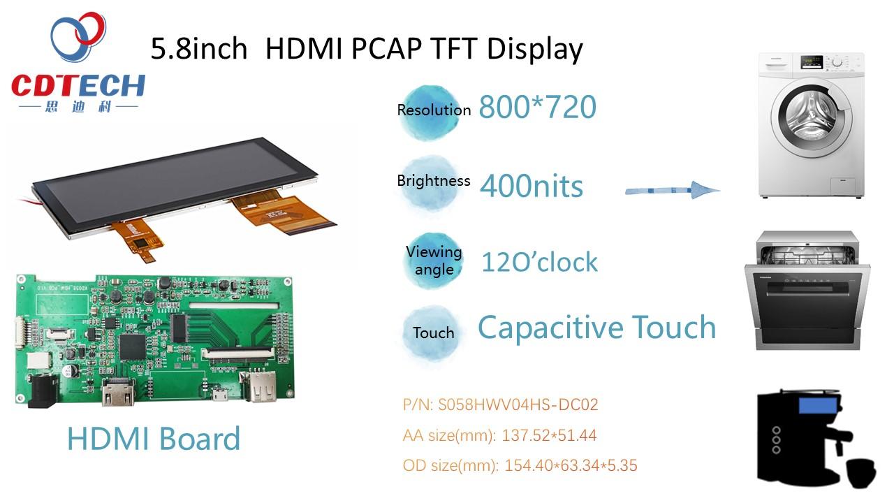


12 O’clock視角 5.8インチバータイプ TFT LCD 800X320 400nits HDMI付き
CDTechは、2011年に設立された中国 深センのTFT液晶ディスプレイ(LCD)、TFT液晶ディスプレイモジュール(LCM)、静電容量式タッチスクリーン、産業用HMIハードウェアのメーカーです。5.8インチバータイプ TFT LCD S058HWV04HS-DC02 のご紹介です。
12 O’clock視角 5.8インチバータイプ TFT LCD 800X320 400nits HDMI付き
型番:S058HWV04HS-DC02
インターフェース:24bit-RGB
光度:400nits
視角:12 O’clock
解像度:800*320
◇メーカーサイト
https://www.cdtech-lcd.com/
このカタログについて
| ドキュメント名 | CDTech (中国) 5.8インチ バータイプ TFT LCD 800X320 S058HWV04HS-DC02 |
|---|---|
| ドキュメント種別 | その他 |
| ファイルサイズ | 1.2Mb |
| 登録カテゴリ | |
| 取り扱い企業 | 二松電気株式会社 (この企業の取り扱いカタログ一覧) |
この企業の関連カタログ


このカタログの内容
Page1
CDTech(H.K.)Electronics Limited
Product Specification
Model Name S058HWV04HS-DC02
Standard LCD Module
Description 5.8" WVGA
800(RGB)x320 Dots
Date 2019/8/26
Version 1.0
Approved Check Prepared
by/Date by/Date by/Date
ZHP 2019/8/26 HZX 2019/8/26 Yigui.Han 2019/8/26
Customer Approval
Date
Page1 of 31
Page2
CDTech(H.K.)Electronics Limited
Table of Contents
1. Record of Revision..............................................................................................................3
2. General Specifications.......................................................................................................4
3. Input/OutputTerminals....................................................................................................... 5
4. Absolute Maximum Rating................................................................................................8
5. Electrical Characteristics.......................................................................................8
6. Interface Timing....................................................................................................12
7. Optical Characteristics....................................................................................................18
8. Environmental / Reliability Tests.................................................................................. 22
9. Mechanical Drawing......................................................................................................... 23
10. Packing...............................................................................................................................24
11. TFT-LCD Module Inspection Criteria......................................................................... 25
12. Precautions for Use of LCD modules........................................................................30
Page2 of 31
Page3
1.Record of Revision
CDTech(H.K.)Electronics Limited
1. Record of Revision
Rev Issued Date Description Editor
1.0 2019/8/26 First Release. Yigui.Han
Page3 of 31
Page4
2.General Specifications
CDTech(H.K.)Electronics Limited
2. General Specifications
Feature Spec
Size 5.8 inch
Resolution 800(horizontal)*320(Vertical)
Interface RGB-24bit
Connect type Connector
Display Colors 16.2M
Technology type a-Si
Characteristics
Pixel pitch (mm) 0.1719 x 0.1607
Pixel Configuration R.G.B.-Stripe
Display Mode Normally White
CTP Driver IC GT5668
Viewing Direction 12 O’clock
Gray Inversion Direction 6 O’clock
LCM (W x H x D) (mm) 154.40*63.34*5.35
Active Area(mm) 137.52 x51.44
Mechanical With /Without TSP With CTP
Weight (g) TBD
LED Numbers 24 LEDs
Note 1: Requirements on Environmental Protection: RoHs
Note 2: LCM weight tolerance: +/- 5%
Page4 of 31
Page5
3.Input/Output Terminals
CDTech(H.K.)Electronics Limited
3. Input/Output Terminals
LCD PIN-MAP
No. Symbol Description
1 AGND System Ground
2 AVDD Analog power
3 VCC Power supply for logic operation
4~11 R0~R7 Data bus
12~19 G0~G7 Data bus
20~27 B0~B7 Data bus
28 DOTCLK Pixel clock signal
29 DE Data Enable
30 HSD Horizontal Sync signal
31 VSD Vertical Sync signal
DE/SYNC mode select. Normally pull high
32 MODE3
H: DE mode. L: HSD/VSD mode
Global reset pin. Active low to enter reset state.
33 RSTB Suggest to connecting with an RC reset circuit for stability.
Normally pull high. (R=47KΩ,C=1μ)
Standby mode, normally pull high
34 STBYB STBYB=”1”, normal operation
STBYB=”0”,timming control, source driver will turn off, all output are high-Z
35 SHLR Left or Right Display Control
36 VCC Digital Power
37 UPDN Up / Down Display Control
38 GND Digital Ground
39 AGND Analog Ground
40 AVDD Analog Power
41 VCOM Common Voltage
Dithering setting
42 DITH DITH=”H” 6bit resolution(last 2 bit of input data truncated) (default setting)
DITH=”L” 8bit resolution
Page5 of 31
Page6
CDTech(H.K.)Electronics Limited
43,44 NC Not connect
45 V10 Gamma correction voltage reference
46 V9 Gamma correction voltage reference
47 V8 Gamma correction voltage reference
48 V7 Gamma correction voltage reference
49 V6 Gamma correction voltage reference
50 V5 Gamma correction voltage reference
51 V4 Gamma correction voltage reference
52 V3 Gamma correction voltage reference
53 V2 Gamma correction voltage reference
54 V1 Gamma correction voltage reference
55 NC Not connect
56 VGH Positive Power for TFT
57 VCC Digital Power
58 VGL Negative Power for TFT
59 GND Digital Ground
60 NC Not connect
BL PIN-MAP
Pin Signal Description
1 LEDA Backlight LED Cathode
2 LEDK Backlight LED Anode
CTP PIN-MAP
Pin Signal Description
1 VSS Ground
2 VDD Power supply(3.3v)
3 SCL I2C clock input(1.8v)
4 VSS Ground
5 SDA I2C data input and output(1.8v)
6 VSS Ground
7 /RST Reset Pin for CTP
8 NC No connect
9 /INT Interrupt request to the host(1.8v)
10 VSS Ground
【Note1】Mating connector:HIROSE, FH28-60S-0.5SH, 60pin,pitch = 0.5mm
【Note2】SHLR:left or right setting
UPDN:up or down setting
Page6 of 31
Page7
4.Absolute Maximum Rating
CDTech(H.K.)Electronics Limited
4. Absolute Maximum Rating
Item Symbol MIN MAX Unit Remark
Supply Voltage VDD -0.5 5.0 V
Operating Temperature TOPR -20 70 ℃
Storage Temperature TSTG -30 80 ℃
Page7 of 31
Page8
CDTech(H.K.)Electronics Limited
5. Electrical Characteristics
5.1 TFT LCD Module
Page8 of 31
Page9
CDTech(H.K.)Electronics Limited
5.2 AC Characteristics
Page9 of 31
Page10
CDTech(H.K.)Electronics Limited
5.3 CTP Electrical Characteristics
FPC Design Item Description Remark
IC solution on TPModel GT5668
Touch Count Max 5 points
COF Display Resolution 800*320
Interface Type I2C
Origin of Coordinate Top left corner
Parameter Symbol Min Typ Max Unit
Interface Signal Voltage VDDI - 1.8 - V
Power Voltage VDD 2.8 - 3.3 V
5.4 LED Driving Conditions
Item Symbol MIN TYP MAX Unit Remark
Forward Current IF - 160 - mA
Forward Voltage VF 8.6 9.6 10.6 V
Backlight Power consumption WBL - 1.536 - W
LED Lifetime - 30000 - Hrs
Note 1: Each LED: IF =20 mA, VF =3.2+/-0.2V.
Note 2: Optical performance should be evaluated at Ta=25℃ only.
Note 3: If LED is driven by high current, high ambient temperature & humidity condition. The life
Time of LED will be reduced. Operating life means brightness goes down to 50% initial brightness.
Typical operating life time is estimated data.
K
A
Figure: LED connection of backlight(Constant Current)
Page10 of 31
Page11
CDTech(H.K.)Electronics Limited
5.5 Block Diagram
R(0:7),G(0:7),
B(0:7),HSN,V
LCD Panel SN,CLK, DEN RGB
888
Source+Gate Driver
5.8 inch F
800(RGB )*320 P
C
Grayscale VDD,GND Power
Manipulation VCOM
Voltage
BLU VLED+,VLED-
BLU
VDD,SCL,SD
A,INT,RST
GND
CTP Panel
Page11 of 31
Page12
CDTech(H.K.)Electronics Limited
6. Interface Timing
6.1 Timing Diagram of Interface Signal
Page12 of 31
Page13
CDTech(H.K.)Electronics Limited
Page13 of 31
Page14
CDTech(H.K.)Electronics Limited
6.2 Power Sequence
Page14 of 31
Page15
CDTech(H.K.)Electronics Limited
6.3 Gamma Circuit
Page15 of 31
Page16
CDTech(H.K.)Electronics Limited
6.3 Capacitive touch panel Specification
Page16 of 31
Page17
CDTech(H.K.)Electronics Limited
Page17 of 31
Page18
7.Optical Characteristics
CDTech(H.K.)Electronics Limited
7. Optical Characteristics
Items Symbol Condition Min. Typ. Max. Unit Remark Note
Transmittance
(With PZ) T 3.77 4.1 - ms FIG.1 Note4-
Contrast Ratio CR 480 600 - - FIG.2 Note1
Surface
luminance LV θ=0° - 400 - cd/m2 FIG.2 Note2
Response Rising TR 2 4
Time θ=0° msec FIG.2 Note3Falling TF 6 12
NTSC - θ=0° - 50 - % FIG.2 Note5
θT - 65 - deg FIG.3
θ
Viewing angle B Center
- 55 - deg FIG.3
θL CR≥10
Note6
- 65 - deg FIG.3
θR - 65 - deg FIG.3
R TBD TBD TBD -
Red X
RY TBD TBD TBD -
G θ=0° TBD TBD TBD -
Green X
GY ∅=0° TBD TBD TBD -Chromaticity FIG.2 Note5
B
Blue X
TBD TBD TBD - CIE1931
Ta=25°
BY TBD TBD TBD -
W
White X
TBD TBD TBD -
WY TBD TBD TBD -
Page18 of 31
Page19
CDTech(H.K.)Electronics Limited
Note1. Definition of contrast ratio
Contrast ratio(Cr) is defined mathematically by the following formula. For more information see FIG.2.
Luminance measured when LCD on the “White” state
Contrast ratio=
Luminance measured when LCD on the “Black” state
For contrast ratio, Surface Luminance, Luminance uniformity and CIE,the testing data is base on TOPCON’s BM-5
or BM-7 photo detector or compatible.
Note2. Definition of surface luminance.
Surface luminance is the luminance with all pixels displaying white. For more information see FIG.2.
Lv = Average Surface Luminance with all white pixels(P1,P2,P3, ......,Pn)
Note3. Definition of luminance uniformity
The luminance uniformity in surface luminance is determined by measuring luminance at each test position 1
through n, and then dividing the maximum luminance of n points luminance by minimum luminance of n points
luminance.For more information see FIG.2.
Minimum surface luminance with all white pixels (P1,P2,P3,......,Pn)
YU=
Maximum surface luminance with all white pixels (P1,P2,P3,......,Pn)
Note4. Definition of response time
The response time is defined as the LCD optical switching time interval between “White” state and
“Black”state.Rise time (Tr) is the time between photo detector output intensity changed from 90% to 10%. And
fall time (Tf) is the time between photo detector output intensity changed from 10% to 90%.
For additional information see FIG1.
Note5. Definition of color chromaticity (CIE1931)
CIE (x,y) chromaticity,The x,y value is determined by screen active area center position P5.For more information
see FIG.2.
Note6. Definition of viewing angle
Viewing angle is the angle at which the contrast ratio is greater than 10. Angles are determined for the horizontal or
x axis and the vertical or y axis with respect to the z axis which is normal to the LCD surface. For more information
see FIG.3.
For viewing angle and response time testing, the testing data is base on Autronic-Melchers’s ConoScope or DMS
series Instruments or compatible.
Page19 of 31
Page20
CDTech(H.K.)Electronics Limited
FIG.1.The definition of response Time
FIG.2. Measuring method for contrast ratio, surface luminance,
luminance uniformity, CIE (x,y) chromaticity
Size : S≤5”(see Figure a) A : 5 mm B : 5 mm
H,V : Active area
Light spot size ∅=5mm(BM-5) or ∅=7.7mm (BM-7)50cm distance or
compatible distance from the LCD surface to detector lens.
test spot position : see Figure a.
measurement instrument : TOPCON’s luminance meter BM-5 or
BM-7 or compatible (see Figure c).
Figure a
Size : 5”<S≤12.3”(see Figure b) H,V : Active area
Light spot size ∅=5mm(BM-5) or ∅=7.7mm (BM-7)50cm distance or
compatible distance from the LCD surface to detector lens.
test spot position : see Figure b.
measurement instrument : TOPCON’s luminance meter BM-5 or
BM-7 or compatible (see Figure c).
BM-5/BM-7
Figure b
Figure c
Page20 of 31