


超高速枚葉式スパッタ装置 SOLARISファミリー
『SOLARISファミリー』は、1枚当たり最速3秒の成膜を可能としたインライン式生産プラットフォームです。
5000台を超える高速光ディスク用システムを納入したノウハウと、
3000台を超える半導体用PVD装置から得られた経験を組み合わせて、
薄膜の大量生産における新しいアプローチを提供。
「完全に自動化された工場」向けに設計されており、スループットを
向上させ、手動処理を排除します。
【特長】
■基板成膜に「インライン」式アーキテクチャを導入
■「完全に自動化された工場」向けに設計
■スループットを向上させ、手動処理を排除
■柔軟性の高いプロセス向けの高速生産ソリューションを提供
※詳しくは関連リンクをご覧いただくか、お気軽にお問い合わせください。
このカタログについて
| ドキュメント名 | SOLARIS |
|---|---|
| ドキュメント種別 | 製品カタログ |
| ファイルサイズ | 2.2Mb |
| 登録カテゴリ | |
| 取り扱い企業 | 日本エバテック株式会社 (この企業の取り扱いカタログ一覧) |
この企業の関連カタログ


このカタログの内容
Page1
SOLARIS
PLATFORMS
Fully automated solutions
for thin film production
Page2
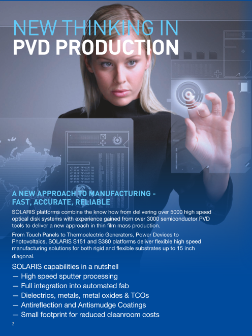
NEW THINKING IN
PVD PRODUCTION
A NEW APPROACH TO MANUFACTURING -
FAST, ACCURATE, RELIABLE
SOLARIS platforms combine the know how from delivering over 5000 high speed
optical disk systems with experience gained from over 3000 semiconductor PVD
tools to deliver a new approach in thin film mass production.
From Touch Panels to Thermoelectric Generators, Power Devices to
Photovoltaics, SOLARIS S151 and S380 platforms deliver flexible high speed
manufacturing solutions for both rigid and flexible substrates up to 15 inch
diagonal.
SOLARIS capabilities in a nutshell
— High speed sputter processing
— Full integration into automated fab
— Dielectrics, metals, metal oxides & TCOs
— Antireflection and Antismudge Coatings
— Small footprint for reduced cleanroom costs
2
Page3
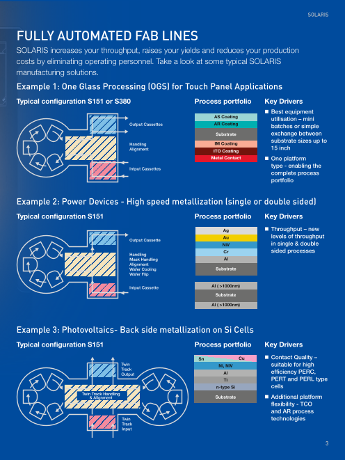
SOLARIS
FULLY AUTOMATED FAB LINES
SOLARIS increases your throughput, raises your yields and reduces your production
costs by eliminating operating personnel. Take a look at some typical SOLARIS
manufacturing solutions.
Example 1: One Glass Processing (OGS) for Touch Panel Applications
Typical configuration S151 or S380 Process portfolio Key Drivers
Best equipment
AS Coating utilisatSionn – mini Cu Ag
Output Cassettes AR Coating batches or simNpi, lNei V Au
exchange betweAel n NiV
Substrate
Output Cassettes substrate sizes uTip to Cr Al ( >1000nm)
Handling IM Coating n-type Si Al
Alignment Substrate
ITO Coating 15 inch
Metal Contact Substrate Substrate
One platform Al ( >1000nm)
Handling
Alignment type - enabling the
Intput Cassettes
Output Cassettes complete process
portfolio
Intput Cassettes
Handling
Example 2: Power Devices - HAliiggnmhe nst peed metallization (single or double sided)
Typical configuration S151 Intput Cassettes Process portfolio Key Drivers
Output Cassette
AS Coating Sn Cu Ag Throughput – new
AR Coating NH levels of throughput
Oai,un Ntpdi
uli
V
tn Cg
Au
assette
MaAslk Handling NiV in single & double
Substrate Alignment
WaTfei r Cooling Cr sided proceAsHandling l s( e>1s000nm)
IM Coating nWM-tyaapsfeker HFSaliipndling Al
AS Coating Substrate
Sn ITO CoatingCu AliAggnment
AR Coating MetNail, CNoiVntact SubAsutrate Substrate
IWafer Cooling
WO
nutpatfpeut r t
C
F C
a
lipa
sssseetttete Al ( >1000nm)
Al NiV
Substrate
Ti IHnatCpnurdtl inCgassette Al ( >1000nm)
IM Coating n-type Si MaAslk Handling
Substrate
ITO Coating Alignment
Metal Contact Substrate SuWbasfterra Cteooling
Wafer Flip Al ( >1000nm)
Twin
TrackIn tput Cassette
Output
Example 3: Photovoltaics- BTwain ck side metallization on Si Cells
Track
Typical configuration S151 Output
Twin Track Handling Process portfolio Key Drivers
& Alignment
AS Coating Sn Cu Contact QualityA –g
Twin Track Handling
& Alignment TwAinR Coating Ni, NiV suitable for highA u
TTrwacink
O efficiency PERC,
Truatput Al NiV
Scukb strate
Input Ti PERT and PERLC trype Al ( >1000nm)
TwIMin Coating n-type Si cells Al
Track Substrate
Twin Track Handling ITO Coating
& Alignment Input
Metal Contact Substrate Additional plaSutfbosrtrmat e Al ( >1000nm)
flexibility - TCO
and AR process
Twin technologies
Track
Input
3
Page4
SOLARIS S151
MAIN FEATURES
— Substrates sizes up to 8 inch diagonal or mini batches
— Single substrate / carrier processing at throughputs up
to 1200 pieces / hour**
— Up to 6 process stations for RTP, PVD, Etch or CVD
SOLARIS S151 carrier for flexible substrate sizes: 3.5” to 8” (max. area Ø220mm)
2” carrier 3.5” carrier 8” carrier 8” carrier
** C ycle times according exact process
Carrier Ø 245mm
Page5
SOLARIS S380
MAIN FEATURES
— Substrates sizes up to 15 inch diagonal or mini batches
— Single substrate / carrier processing at throughputs
up to 900 pieces/hour**
— Up to 5 process stations for RTP, PVD, Etch or CVD
SOLARIS S380 carrier for flexible substrate sizes: 3.5” to 15” (max. area Ø380mm)
8” carrier 12” carrier 15” carrier EMI carrier
** C ycle times according exact process
Carrier Ø 430mm
Page6
THE POWER
BEHIND SOLARIS
SOLARIS SUBSTRATE
HANDLING -
SPEED AND FLEXIBILITY
Whether you choose the S151 or S380 platform you
can handle glass, silicon or polymeric substrates
with ease. Parallel carrier transfer around SOLARIS
by synchronous indexer is the perfect solution to
achieve high speed processing and lowest cost of
ownership in mass production applications.
— Carriers for individual substrates or mini
batches without compromise on process
uniformity
— Simple conversion between rigid,
2.5D substrates & foils
— Make multiple passes in front of process
stations for complex stack designs
— Change direction of indexer travel enabling
sputter in reverse order for more process
flexibility
6
Page7
SOLARIS
SOURCE TECHNOLOGY
From EMI shielding applications to Thermoelectric Generators,
SOLARIS brings you advanced source technologies for
deposition of metals, alloys, oxides, dielectrics and TCOs.
SOLARIS SOURCE TECHNOLOGY -
SPEED WITHOUT COMPROMISE
IN FILM QUALITY
Choose from large area single DC, DC Reactive or RF sputter
with cooling, etch and RTP capabilities up to 550ºC , or
Evatec multisource capability for up to 4 sputter cathodes
at a single process station. All process modules run
independently in isolation and are configured according to
your application.
— Dielectrics: SiN-H, SiN, SiO2, Al2O3, SiC
— Metal Oxides: NbO2, TiO2, Ta2O5
— TCOs: ITO, GZO, Zn:AlO
— Metal stacks: Al, NiV, Ag, AuGe
— Alloys with MSQ multisource
— Deposition uniformities <±2% over whole carrier
PENTA PLUS
CATHODE
TECHNOLOGY
Penta Plus cathode technology
delivers perfect step coverage
in deposition of alloys in EMI
shielding and reduces both
consumables costs and target
change times
7
Page8
SOLARIS Platform summary
Fully automated production solutions
From Touch Panels to Thermoelectric Generators, Power
Devices to Photovoltaics, SOLARIS platforms deliver High-throughput on substrates sizes up to 15” diagonal
flexible high speed manufacturing solutions. Flexible configurations
TYPICAL LAYOUTS
SOLARIS S380
SOLARIS S151
ABOUT EVATEC
Evatec offers complete solutions for thin film deposition Our team is ready to offer process advice, sampling
and etch in the semiconductor, optoelectronics and services and custom engineering to meet our customers
photonics markets. individual needs in platforms from R&D to prototyping and
true mass production.
Our technology portfolio includes standard and enhanced
evaporation, a range of advanced sputter technologies as We provide sales and service through our global network
well as plasma deposition & etch. of local offices.
For more information visit us at www.evatecnet.com or contact our head office.
Evatec AG Tel: + 41 81 403 80 00 Product descriptions, photos and data are supplied within the
brochure for general information only and may be superseded
Hauptstrasse 1a Fax: + 41 81 403 80 01 by any data contained within Evatec quotations, manuals or
CH-9477 Trübbach info@evatecnet.com specifications.
Edition 3: Reprinted March 2018, first printed June 2017.
Switzerland www.evatecnet.com (Edition 2 first printed Jan 2016, Edition 1 first printed Sep 2015).
EVA_Brochure_SOLARIS_Edition3_March2018