


P R E C I S I O N C E R AMI C S
掲載製品
・静電チャック
・プラズマ耐性部品
・半導体チャンバー構造部品
・多孔質セラミック真空チャック/キャリア
・アルミナセラミック基板
・窒化アルミニウムセラミック基板
・セラミックロボットチャック
・太陽光発電用真空チャック
・窒化ケイ素セラミック基板
・ジルコニアセラミックプレート
・液晶平面用セラミックプレート
このカタログについて
| ドキュメント名 | 精密セラミックス |
|---|---|
| ドキュメント種別 | 製品カタログ |
| ファイルサイズ | 2.3Mb |
| 登録カテゴリ | |
| 取り扱い企業 | ハポイン株式会社 (この企業の取り扱いカタログ一覧) |
この企業の関連カタログ


このカタログの内容
Page1
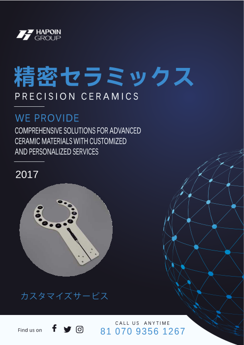
精密セラミックス
P R E C I S I O N C E R A M I C S
WE PROVIDE
COMPREHENSIVE SOLUTIONS FOR ADVANCED
CERAMIC MATERIALS WITH CUSTOMIZED
AND PERSONALIZED SERVICES
2017
カスタマイズサービス
C A L L U S A N Y T I M E
Find us on 81 070 9356 1267
01
Page2
Company profile
会社概要
ハポイングループは1999年に設立され、本社は上海にあります。深圳、香港、ハノイにも
支社を設置しています。2017年には、日本・東京に支社を設立しました。
衡鹏(HAPOIN)グループは常に、国際的な先端技術、高度な製造装置、重要な生産材料の
提供に力を注いできました。20年以上にわたる発展と蓄積を経て、同グループは自社の技
術開発チーム、生産設備、部品製造工場を有しています。
衡鹏グループは、半導体業界および電子組立業界における精密セラミックス、高度な製造装
置、部品および消耗品などの製品に注力しています。
衡鹏グループは、その強力な事業ネットワークと豊富な国際貿易経験を活かして、日本のお
客様に最適なソリューションを提供することを目指しています。お客様の業務ニーズに迅速
に対応し、高品質で信頼性の高い製品を安定供給することで、長期的なパートナーシップの
構築に尽力しています。
Hapoin group was established in 1999 and is headquartered in Shanghai. We also have
branches in shenzhen, Hong Kong and Hanoi. In 2017, we opened a branch office in Tokyo,
Japan.
Hapoin group has always been committed to providing international cutting-edge technolo-
gy, advanced manufacturing equipment and important production materials. After more than
20 years of development and accumulation, the group has its own technology development
team, production facilities and parts manufacturing plants.
Hongpeng group focuses on precision ceramics, advanced manufacturing equipment,
components and consumables in the semiconductor and electronic assembly industries.
Utilizing its strong business network and rich international trade experience, hengpeng group
aims to provide the best solutions for Japanese customers. We are committed to building
long-term partnerships by responding quickly to our customers' business needs and ensuring
a stable supply of high-quality and reliable products.
Page3
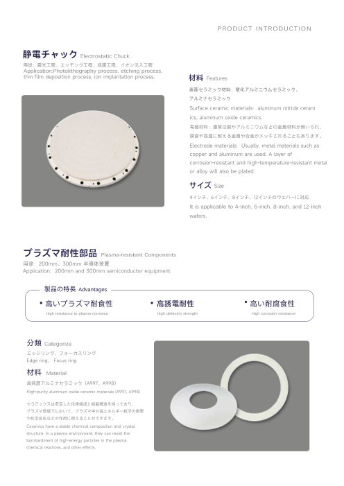
PRODUCT INTRODUCTION
静電チャック E l e ct r o st a ti c Chuck
用途:露光工程、エッチング工程、成膜工程、イオン注入工程
Application:Photolithography process, etching process,
thin film deposition process, ion implantation process. 材料 Features
表面セラミック材料:窒化アルミニウムセラミック、
アルミナセラミック
Surface ceramic materials: aluminum nitride ceram
ics, aluminum oxide ceramics.
電極材料:通常は銅やアルミニウムなどの金属材料が用いられ、
腐食や高温に耐える金属や合金がメッキされることもあります。
Electrode materials: Usually, metal materials such as
copper and aluminum are used. A layer of
corrosion-resistant and high-temperature-resistant metal
or alloy will also be plated.
サイズ Size
4インチ、6インチ、8インチ、12インチのウェハーに対応
It is applicable to 4-inch, 6-inch, 8-inch, and 12-inch
wafers.
プラズマ耐性部品 Plasma-resistant Components
用途:200mm、300mm 半導体装置
Application: 200mm and 300mm semiconductor equipment
製品の特長 Advantages
● 高いプラズマ耐食性 ● 高誘電耐性 ● 高い耐腐食性
High resistance to plasma corrosion High dielectric strength High corrosion resistance
分類 Categorize
エッジリング、フォーカスリング
Edge ring、 Focus ring
材料 Material
高純度アルミナセラミック(A997、A998)
High-purity aluminum oxide ceramic materials (A997, A998)
セラミックスは安定した化学組成と結晶構造を持っており、
プラズマ環境下において、プラズマ中の高エネルギー粒子の衝撃
や化学反応などの作用に耐えることができます。
Ceramics have a stable chemical composition and crystal
structure. In a plasma environment, they can resist the
bombardment of high-energy particles in the plasma,
chemical reactions, and other effects.
Page4
PRODUCT INTRODUCT ION
半導体チャンバー構造部品 Semiconductor Chamber Structural Parts
用途:半導体PVD、CVD、ETCHチャンバー材料
Key components of PVD, CVD, and ETCH chambers in semiconductor processes.
製品の特長
Advantages
◎ 耐食性
◎ 絶縁性
◎ プラズマ耐性に優れる
Corrosion Resistance
Insulation
Plasma Resistance.
材料純度 Material Purity 加工可能寸法 Dimension Specifications
99.7%,99.8%,99.9% アルミナ 円盤φ650mm(長尺物は2000mm)まで対応可能
99.7%, 99.8%, 99.9% Alumina. Disc diameter within φ650mm (or strips up to 2000mm in length).
加工技術 Processing Methods 精度保証 Precision Range
静水圧プレス成形、焼結、精密加工対応 寸法公差±0.01mm、平面度最高0.002mm、表面粗さRa0.2
Isostatic pressing, sintering, precision Dimensional tolerance ±0.01mm; flatness up to 0.002mm,
machining, etc. surface roughness Ra0.2.
多孔質セラミック真空チャック/キャリア Microporous Ceramic Vacuum Chuck/Carrier
产品优势 Advantages
● 高硬度 ● 放熱性 ● 耐摩耗 ● 耐酸・耐アルカリ、耐腐食
High Hardness Rapid Heat Excellent Wear Strong Resistance To Acid, Alkali, And Corrosion, Adaptable To Extremely
Dissipation Resistance H arsh Environments.
用途 Application Scenarios
1、半導体工程でのウェハー薄化、切断、研磨、洗浄などにおける固
定治具ます。
Used as a workbench (fixed fixture) in the semiconductor industry
during processes such as wafer thinning, shaping, slicing,
grinding, and cleaning.
2、材料内部に高温焼結で形成された均一な多孔構造により、真空吸
着を通じて半導体ウェハーなどを確実に固定します。
Through high-temperature sintering, a large number of intercon-
nected or closed uniform solid or vacuum ceramic structures are
formed within the material. These utilize vacuum suction to fix
semiconductor wafers or other workpieces in place.
Page5
PRODUCT INTRODUCT ION
アルミナセラミック基板 Alumina Ceramic Substrate
用途:電子部品の放熱基板、自動車用パワー回路基板、プリンター、LED照明、通信機器
Widely used in electronic component heat dissipation substrates, high-power circuit boards in the automotive industry,
copper-clad boards, printers, LED lighting, and communication devices.
材料号 Material Grades
92%、96%、98%、99%、99.5%酸化アルミ
92%, 96%, 98%, 99%, 99.5% Alumina.
加工方法 Processing Methods
レーザーマーキング、金型プレス
Laser scribing, mold stamping.
厚さ Thickness Range
0.2mm 、3.0mm
Minimum 0.2mm, maximum 3.0mm.
孔径 Dimensions
長さ最大 420mm、幅 240mm
Maximum length 420mm, maximum width 240mm.
孔径范围 Hole Diameter Range
最小孔径φ0.07mm
Minimum hole diameter φ0.07mm.
特長 Advantages
● 優れた熱伝導性と耐熱衝撃性を備える ● 表面特性と平滑性が高く、寸法精度にも優れている ● 耐腐食性があり
Excellent thermal conductivity and thermal Superior surface properties, flatness, and high Corrosion resistance
shock resistance dimensional accuracy
● 物理的および化学的性質は安定している ● 高い絶縁性能、低い誘電率と誘電損失 ● そして優れ た機械的強度を有している
Stable physical and chemical properties High insulation performance, low dielectric constant, Excellent mechanical strength
and low dielectric loss
窒化アルミニウムセラミック基板 Aluminum Nitride Ceramic Substrate
用途:放熱、LEDパッケージ、半導体、薄膜回路、パワーレジスタ基板
Heat dissipation substrates, led packaging substrates, semiconductor substrates, thin film circuit substrates, and
Power resistor substrates.
製品の特長 Advantages
1、熱伝導率 > 170W/m・(アルミナの約7倍)、酸化アルミニウムよりも優れた機械
的強度を有している
The thermal conductivity is greater than 170 W/m·K, which is over 7 times higher than that
of aluminum oxide; it also has better mechanical strength compared to aluminum oxide.
2、高強度、高電気絶縁性、低誘電率、低損失
It possesses high electrical insulation, with a low dielectric constant and low dielectric loss.
3、シリコンに近い熱膨張係数、大型シリコンチップの搭載と熱サイクルに対して、
高い信頼性を実現している
It has a thermal expansion coefficient similar to that of silicon, ensuring high reliability for
mounting large silicon chips and thermal cycling.
4、融解状態な金属に対して優れた耐食性を有している
It has good corrosion resistance to molten metals.
5、不純物の含有量は極めて少なく、無毒で、高い純度を誇り
It contains minimal impurities, is non-toxic, and has high purity.
Page6
PRODUCT INTRODUCT ION
セラミックロボットチャック Ceramic Robotic Fork
用途:主に半導体装置で搬送搬送の役割を果たします。半導体装置というロボットの「手」に相当し、
ウエハ/シリコンのウェハを所定の位置に搬送する役割を担います。
Primarily used in semiconductor equipment for transportation and handling. It serves as the "hand" of the robot
in semiconducto machines, responsible for moving wafers/silicon chips to designated positions.
材料 Material
99.7% アルミナセラミック。高密度、高硬度、高耐摩耗性、耐熱性、絶縁性、耐腐食性を備える
99.7% alumina ceramic, featuring high density, high hardness, excellent wear resistance, superior heat resistance, outstanding
mechanical strength, stable insulation performance at high temperatures, and excellent corrosion resistance.
利点 Advantages
ウェハーの表面を傷つけない、汚染防止、破損防止
Prevents scratches on the surface of wafers/silicon chips, Avoids contamination from other substances, Prevents damage to the
components.
太陽光発電用真空チャック Photovoltaic Vacuum Suction Cups
製品の特長
Advantages
◎ 高耐熱性
◎ 耐腐食性
◎ 絶縁性
◎ 耐摩耗性
High Temperature Resistance
Corrosion Resistance
Insulation
Wear Resistance
Page7
PRODUCT INTRODUCT ION
窒化ケイ素セラミック基板 Silicon Nitride Substrate
用途:放熱基板、パワーエレクトロニクス回路基板
Heat Dissipation Substrate, Power Electronic Circuit Substrate
特長 Features
1、アルミナ基板または窒化アルミ基板と比較して、約2
倍以上の曲げ強度を有している
Compared with aluminum oxide substrates or alumi-
num nitride substrates, it has more than twice the
bending strength.
2、アルミナ基板またはZTA基板と比較して、3倍以上の
熱伝導率を有している
Compared with alumina substrates or ZTA substrates,
it has more than three times the thermal conductivity.
3、高絶縁性
High electrical insulation
4、熱膨張はシリコンに近い
Thermal expansion coefficient similar to silicon
ジルコニアセラミックプレート Zirconia Ceramic Board
用途:機械設備、太陽光、航空宇宙、医療、石油加工
Widely Used In Mechanical Equipment, Solar Photovoltaic, Aerospace, Medical Industry,
Petroleum Processing, And More.
特長 Advantages
● 耐高温 ● 耐腐食 ● 耐摩耗
High Temperature Resistance Corrosion Resistance Wear Resistance
加工方法:乾式圧縮、等方圧成形
Ceramic board, formed by dry pressing and isostatic pressing
processes.
テープキャスティング
Ceramic sheet, formed by the casting process.
サイズ Specification
最大400×400mm、最小厚み0.15mm
The maximum size can be 400mm x 400mm, and the
minimum thickness can be 0.15mm.
顧客仕様によりカット可能
It can be cut into different widths according to the customer's
actual requirements.
Page8
PRODUCT INTRODUCT ION
液晶平面用セラミックプレート Applied liquid crystal planar ceramic plate
用途:液晶パネル用部品
Purpose: Accessories for liquid crystal flat panels
材質 Material
99.8%Al2O3セラミック材料
99.8% Al₂O₃ ceramic material
寸法規格 Size specification
最大加工長≤2000 mm
Length ≤ 2000 mm
図面に基づく精密加工/製品
リバースエンジニアリング加工対応
Processed according to the drawing、
Processed based on product surveying
and mapping
製品の特長 Advantages
● 耐落下 ● 耐沖突 ● 耐スクラッチ ● 洗浄しやすい ● 防潮性
Drop-resistant Impact-resistant Scratch-resistant Easy To Clean Moisture Resistance
● 耐摩耗性 ● 防火性 ● 耐化学腐蚀 ● 静電気 ● 抗紫外線
Wear-resistant Fire Resistance Chemical Corrosion Resistance Anti-static Ultraviolet Resistance
セラミック移印刀 Zirconia Ceramic Board
応用: 電子業界、玩具メーカー、日用品業界、自動車部品メーカー、医療業界
Widely Used In Mechanical Equipment, Solar Photovoltaic, Aerospace, Medical Industry,
Petroleum Processing, And More.
製品の特長
Advantages
◎ 高硬度
◎ 良好な耐摩耗性
◎ 化学的安定性
◎ 高強度と靭性
High hardness
Good wear resistance
Chemical stability
High strength and toughness
Page9
◎日本 Japan
◎上海 Shanghai
深セン Shengzhen◎
香港 Hongkong◎ ◎台湾 Taiwan
◎ベトナム Vietnam
衡鹏精密电子工业(上海)有限公司
Hapoin Precision Electronics Industry(Shanghai)Co., Ltd
上 海市闵行区金都路1165弄南方都市园6号楼
Building 6, Nanfang Urban Park, Lane 1165, Jindu Road, Minhang District, Shanghai, China
Tel: +86 021 6088 8500
E-mail: info@hapoin.com
Web: www.hapoinceramic.com