


アイスモス・テクノロジーのICE11N70FP は11A,700VのTO220 Full Pak パッケージ です。LEDマネージメントに最適です。
【特長】
■TO220Full Pakパッケージ
■低オン抵抗
■超低ゲート電荷重
■耐高dv/dt
■高いUIS特性
■耐高ピーク電流
■増相互コンダクタンス・パフォーマンス
このカタログについて
| ドキュメント名 | ICE11N70FP データシート |
|---|---|
| ドキュメント種別 | 製品カタログ |
| ファイルサイズ | 476.3Kb |
| 登録カテゴリ | |
| 取り扱い企業 | アイスモス・テクノロジー・ジャパン株式会社 (この企業の取り扱いカタログ一覧) |
この企業の関連カタログ


このカタログの内容
Page1
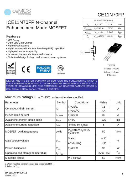
ICE11N70FP
ICE11N70FP Product Summary
N-Channel ID TC=25oC 11A Max
Enhancement Mode MOSFET V(BR)DSS ID=250uA 700V Min
rDS(on) VGS=10V 0.24Ω Typ
Features Qg VDS=480V 81nC Typ
• Low rDS(on)
• Ultra Low Gate Charge D
• High dv/dt capability
• High Unclamped Inductive Switching (UIS) capability
• High peak current capability G
• Increased transconductance performance
• Optimized design for high performance power systems
S
T0220FP
Isolated (T0-220)
1=Gate, 2=Drain,
3=Source.
ICEMOS AND ITS SISTER COMPANY 3D SEMI OWN THE FUNDAMENTAL PATENTS
FOR SUPERJUNCTION MOSFETS. THE MAJORITY OF THESE PATENTS HAVE 17 to 20
YEARS OF REMAINING LIFE. THIS PORTFOLIO HAS GRANTED PATENTS ISSUED IN
USA, CHINA, KOREA, JAPAN, TAIWAN & EUROPE.
Maximum ratings b at Tj=25oC, unless otherwise specified
Parameter Symbol Conditions Value Unit
Tc=25oC 11
Continuous drain current ID A
Tc=100oC 4.4
Pulsed drain current ID, pulse Tc=25oC 35 A
Avalanche energy, single pulse E AS ID=5A 125 mJ
Avalanche current, repetitive I AR limited by Tjmax 5 A
VDS=480V, ID=11A,
MOSFET dv/dt ruggedness dv/dt 5
Tj=125o 0 V/ns
C
Static ±20
Gate source voltage VGS V
AC (f>1Hz) ±30
Power dissipation Ptot Tc=25oC 35 W
o
Operating and storage temperature Tj, Tstg -55 to +150 C
Mounting torque M 3 screws 50 Ncm
a When mounted on 1inch square 2oz copper clad FR-4
b limited by Tjmax
SP-11N70FP-000-11 1
11/10/2022
Page2
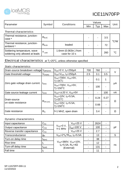
ICE11N70FP
Values
Parameter Symbol Conditions Unit
Min Typ Max
Thermal characteristics
Thermal resistance, junction- R
case thJC
a - - 3.5
oC/W
Thermal resistance, junction- R leaded
ambient thJA
a - - 72
Soldering temperature, wave T 1.6mm (0.063in.) from
soldering only allowed at leads sold case for 10 s - - 260 oC
Electrical characteristics at Tj=25oC, unless otherwise specified
Static characteristics
Drain-source breakdown voltage V(BR)DSS VGS=0 V, ID=250µA 700 760 -
V
Gate threshold voltage VGS(th) VDS=VGS, ID=250µA 2.5 3.1 3.5
VDS=700V, VGS=0V,
T o .1 1
j=25 C - 0
Zero gate voltage drain current IDSS µA
VDS=700V, VGS=0V,
- 00 -
Tj=150o 1
C
Gate source leakage current IGSS VGS=±20 V, VDS=0V - - 100 nA
VGS=10V, ID=5.5A,
-
T 4 0.27
Drain-source j=25oC 0.2
on-state resistance RDS (on) Ω
VGS=10V, ID=5.5A,
-
T 0.66 -
j=150oC
Gate resistance RG f=1 MHZ, open drain - 3.4 - Ω
Dynamic characteristics
Input capacitance Ciss VDS=25 V - 2624 -
V
Output capacitance C GS=0 V,
oss V =100 V - 100 -
f=1 MHz DS pF
Reverse transfer capacitance Crss VDS=25 V - 2.7 -
Transconductance gfs VDS>2*ID*RDS, ID=5.5A - 13 - S
Turn-on delay time td(on) - 38 -
Rise time t VDS=380V, VGS=10V,
r - 12 -
ID=5.5A, RG=4Ω ns
Turn-off delay time td(off) (External) - 131 -
Fall time tf - 11 -
SP-11N70FP-000-11 2
11/10/2022
Page3
ICE11N70FP
Values
Parameter Symbol Conditions Unit
Min Typ Max
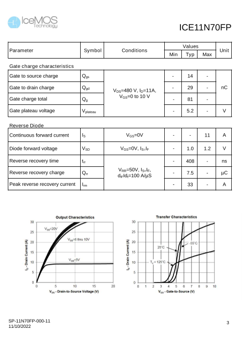
Gate charge characteristics
Gate to source charge Qgs - 14 -
Gate to drain charge Qgd V V, I - nC
DS=480 D=11A, 29 -
Gate charge total Q VGS=0 to 10 V
g - 81 -
Gate plateau voltage Vplateau - 5.2 - V
Reverse Diode
Continuous forward current IS VGS=0V - - 11 A
Diode forward voltage VSD VGS=0V, IS=IF - 1.0 1.2 V
Reverse recovery time trr - 408 - ns
V
Reverse recovery charge Q RR=50V, IS=IF,
rr -
d 7.5 - µC
iFIdt=100 A/µS
Peak reverse recovery current Irm - 33 - A
SP-11N70FP-000-11 3
11/10/2022
Page4
ICE11N70FP
SP-11N70FP-000-11 4
11/10/2022
Page5
ICE11N70FP
SP-11N70FP-000-11 5
11/10/2022
Page6
ICE11N70FP
Package Outline: TO-220 FullPAK
SP-11N70FP-000-11 6
11/10/2022
Page7
ICE11N70FP
Package Outline: TO-220 FullPAK
SP-11N70FP-000-11 7
11/10/2022
Page8
ICE11N70FP
ICEMOS SUPERJUNCTION PATENT PORTFOLIO
ICEMOS GRANTED PATENTS
US7,429,772
US7,439,178
US7,446,018
US7,579,607
US7,723,172
US7,795,045
US7,846,821
US7,944,018
US8,012,806
US8,030,133
3D SEMI PATENTS LICENSED TO ICEMOS
US7,041,560B2
US7,023,069B2
US7,364,994
US7,227,197B2
US7,304,944B2
US7,052,982B2
US7,339,252
US7,410,891
US7,439,583
US7,227,197B2
US6,635,906
US6,936,867
US7,015,104
US9,109,110
US7,271,067
US7,354,818
US7,052,982,
US7,199,006B2
Note: additional patents in China, Korea, Japan, Taiwan, Europe have also been granted to IceMOS and 3D Semi for
Superjunction MOSFETs with 70 additional Patent applications in process in the USA and the above listed countries.
SP-11N70FP-000-11 8
11/10/2022
Page9
ICE11N70FP
Marking Information
YY = Last two digits of the year
WW = Work week
* = Site ID YYWW *
XXXXX
ICE11N70
XXXXX = Lot ID
ICE11N70 = ICE is IceMOS logo and
11N70 is a designated device part
number
Disclaimer
Information contained in this data sheet shall in no event be regarded as a guarantee of conditions or
characteristics. All product, data sheet are subject to change without notice to improve reliability.
ICEMOS technology will not be responsible for damages of any nature resulting from the use or reliance
upon the information contained in this data sheet.
SP-11N70FP-000-11 9
11/10/2022