


ITC576Aは、IMAGICA社のCMOSコンタクトイメージセンサです。576画素、1200dpi/maxで、データレート40MHz/maxの高速駆動が可能ですので、ドキュメントスキャナ、コピー機等の用途に最適です。ITC576Aはウェハーの状態で供給されますので、お客様側でダイシングとアッセンブリをできることが条件となります。1枚のウェハーから、約5000個のダイを取得することができます。
このカタログについて
| ドキュメント名 | ドキュメントスキャナ・コピー機用コンタクトイメージセンサ |
|---|---|
| ドキュメント種別 | 製品カタログ |
| ファイルサイズ | 865.8Kb |
| 登録カテゴリ | |
| 取り扱い企業 | マイクロン株式会社 (この企業の取り扱いカタログ一覧) |
この企業の関連カタログ


このカタログの内容
Page1
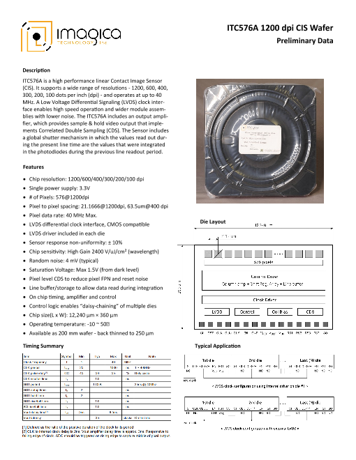
ITC576A 1200 dpi CIS Wafer
Preliminary Data
Description
ITC576A is a high performance linear Contact Image Sensor
(CIS). It supports a wide range of resolutions - 1200, 600, 400,
300, 200, 100 dots per inch (dpi) - and operates at up to 40
MHz. A Low Voltage Differential Signaling (LVDS) clock inter-
face enables high speed operation and wider module assem-
blies with lower noise. The ITC576A includes an output ampli-
fier, which provides sample & hold video output that imple-
ments Correlated Double Sampling (CDS). The Sensor includes
a global shutter mechanism in which the values read out dur-
ing the present line time are the values that were integrated
in the photodiodes during the previous line readout period.
Features
• Chip resolution: 1200/600/400/300/200/100 dpi
• Single power supply: 3.3V
• # of Pixels: 576@1200dpi
• Pixel to pixel spacing: 21.1666@1200dpi, 63.5um@400 dpi
• Pixel data rate: 40 MHz Max.
• LVDS differential clock interface, CMOS compatible Die Layout
• LVDS driver included in each die
• Sensor response non-uniformity: ± 10%
• Chip sensitivity: High Gain 2400 V/uJ/cm² (wavelength)
• Random noise: 4 mV (typical)
• Saturation Voltage: Max 1.5V (from dark level)
• Pixel level CDS to reduce pixel FPN and reset noise
• Line buffer/storage to allow data read during integration
• On chip timing, amplifier and control
• Control logic enables “daisy-chaining” of multiple dies
• Chip size(L x W): 12,240 µm × 360 µm
• Operating temperature: -10 ~ 50℃
• Available as 200 mm wafer - back thinned to 250 µm
Timing Summary Typical Application
Page2
ITC576A 1200 dpi CIS Wafers
Preliminary Data
Normalized Quantum Efficiency
Complete electro-optical performance
data will be available upon completion of
first lot evaluation.
Wafer Configuration
• 200 mm (8-inch) diameter with notch
• 254 µm thickness, background
Pad Functions and Locations Wafer Shot Map
No performance guarantees are made by this
document. All specifications are subject to
change without notice at the sole discretion
of the manufacturer.
Pad size is 95 x 95 µm.
Full specifications available upon execution of a Non-Disclosure Agreement
Manufactured by: Distributed Globally by:
Imagica Technology, Inc. Maxwell-Hiqe Corporation
Vancouver, BC , Canada Tucson, AZ, USA
www.imagica.technology www.maxwell-hiqe.com
L0510001 Sep2018