


工業製品向け 1024*768 8インチ液晶ディスプレイ S080QXG04EA-DC26 の仕様書
型番:S080QXG04EA-DC26
インターフェース:LVDS
バックライト:27 LEDs
光度:800nits
視角:Full view
解像度:1024(horizontal)*768(Vertical)
ODサイズ:183.2*141.09*8.27
AAサイズ:162.05x 121.54
作業温度:-10~+50℃
保存温度:-20~+60℃
◇メーカーサイト
https://www.cdtech-lcd.com/
このカタログについて
| ドキュメント名 | CDTech (中国) 工業製品用 8インチ液晶ディスプレイ S080QXG04EA-DC26 |
|---|---|
| ドキュメント種別 | 製品カタログ |
| ファイルサイズ | 869Kb |
| 登録カテゴリ | |
| 取り扱い企業 | 二松電気株式会社 (この企業の取り扱いカタログ一覧) |
この企業の関連カタログ


このカタログの内容
Page1
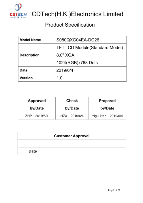
CDTech(H.K.)Electronics Limited
Product Specification
Model Name S080QXG04EA-DC26
TFT LCD Module(Standard Model)
Description 8.0" XGA
1024(RGB)x768 Dots
Date 2019/6/4
Version 1.0
Approved Check Prepared
by/Date by/Date by/Date
ZHP 2019/6/4 HZX 2019/6/4 Yigui.Han 2019/6/4
Customer Approval
Date
Page1 of 27
Page2
CDTech(H.K.)Electronics Limited
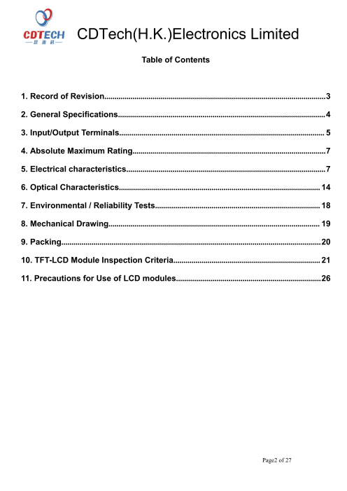
Table of Contents
1. Record of Revision..............................................................................................................3
2. General Specifications.......................................................................................................4
3. Input/Output Terminals...................................................................................................... 5
4. Absolute Maximum Rating................................................................................................7
5. Electrical characteristics...................................................................................................7
6. Optical Characteristics....................................................................................................14
7. Environmental / Reliability Tests.................................................................................. 18
8. Mechanical Drawing......................................................................................................... 19
9. Packing.................................................................................................................................20
10. TFT-LCD Module Inspection Criteria.........................................................................21
11. Precautions for Use of LCD modules........................................................................26
Page2 of 27
Page3
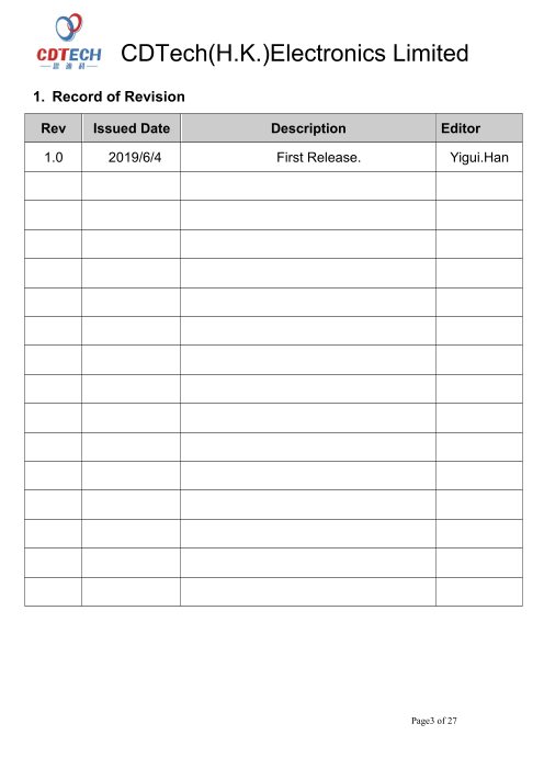
1.Record of Revision
CDTech(H.K.)Electronics Limited
1. Record of Revision
Rev Issued Date Description Editor
1.0 2019/6/4 First Release. Yigui.Han
Page3 of 27
Page4
2.General Specifications
CDTech(H.K.)Electronics Limited
2. General Specifications
Feature Spec
Size 8.0 inch
Resolution 1024(horizontal)*768(Vertical)
Interface LVDS
Connect type Connector
Display Colors 16.7M
Technology type a-Si
Characteristics
Pixel pitch (mm) 0.1583*0.1583
Pixel Configuration R.G.B.-Stripe
Display Mode Normally Black
Driver IC TBD
CTP Driver IC ILI2511
Viewing Direction Full view
LCM (W x H x D) (mm) 183.2*141.09*8.27
Active Area(mm) 162.05*121.54
Mechanical With /Without TSP With CTP
Weight (g) TBD
LED Numbers 27 LEDS
Note 1: Requirements on Environmental Protection: RoHs
Note 2: LCM weight tolerance: +/- 5%
Page4 of 27
Page5
3.Input/Output Terminals 、 LCD PIN-MAP
CDTech(H.K.)Electronics Limited
3. Input/Output Terminals
LCD PIN-MAP
No. Symbol Description
1 VCOM Common voltage
2 VDD 3.3V Power
3 VDD 3.3V Power
4 NC Not connect
Global reset pin Active low enter reset state Suggest to
5 RESET connecting with an
RC reset Normally pull hight(R=100K,C=1UF)
6 STBYB Standby mode normally pull high STBYB=”1”,timingcontrol ,source driver will turn off all output are high-Z
7 GND System Ground
8 RXIN0- Negative LVDS differential data input
9 RXIN0+ Positive LVDS differential data input
10 GND System Ground
11 RXIN1- Negative LVDS differential data input
12 RXIN1+ Positive LVDS differential data input
13 GND System Ground
14 RXIN2- Negative LVDS differential data input
15 RXIN12+ Positive LVDS differential data input
16 GND System Ground
17 RXCLK- Negative LVDS differential clock input
18 RXCLK+ Positive LVDS differential clock input
19 GND System Ground
20 RXIN3- Negative LVDS differential data input
21 RXIN3+ Positive LVDS differential data input
22 GND System Ground
23 NC Not connect
24 NC Not connect
25 GND System Ground
26 NC Not connect
27 DIMO Backlight CABC controller signal output
28 SELB 6bit/8bit mode select H:6bit /L:8bit Note1
29 AVDD Power for Analog Circuit
30 GND System Ground
31 NC(LED-) Not connect
32 NC(LED-) Not connect
Page5 of 27
Page6
CDTech(H.K.)Electronics Limited
33 L/R Horizontal inversion Note3
34 U/D Vertical inversion Note3
35 VGL Positive power for TFT
36 CABCEN1 CABC H/W enable Note2
37 CABCEN0 CABC H/W enable Note2
38 VGH Positive power for TFT
39 NC(LED+) Not connect
40 NC(LED+) Not connect
I: input, O: output, P: Power
Note1: If LVDS input data is 6 bits, selb must be set to High;
If LVDS input data is 8 bits, selb must be set to Low.
Note2: When CABC_EN=”00”, CABC OFF.
When CABC_EN=”01”, user interface image.
When CABC_EN=”10”, still picture.
When CABC_EN=”11”, moving image.
When CABC off, don’t connect DIMO, else connect it to backlight.
Note3: When L/R=”0”, set right to left scan direction.
When L/R=”1”, set left to right scan direction.
When U/D=”0”, set top to bottom scan direction.
When U/D=”1”, set bottom to top scan direction.
CTP PIN-MAP
Pin Signal Description
1 GND Ground
2 D+ Positive voltage data line
3 D- Negative voltage data line
4 VDD(5V) Power supply (5v)
BL PIN-MAP
1 LEDA LED Cathode
2 LEDK LED Anode
Page6 of 27
Page7
4.Absolute Maximum Rating、5.Electrical characteristics
CDTech(H.K.)Electronics Limited
4. Absolute Maximum Rating
Item Symbol MIN Typ MAX Unit Remark
Supply Voltage VDD -0.3 - 5 V -
Operating Temperature TOPR -10 - 50 ℃ -
Storage Temperature TSTG -20 - 60 ℃
5. Electrical characteristics
5.1 Driving TFT LCD Panel
Item Symbol MIN TYP MAX Unit Remark
VCC 3.0 3.3 3.6 V -
AVDD 9.8 10 10.2 V -
Power voltage
VGH 18.6 18.9 19.2 V -
VGL 8.1 7.8 7.5 V -
Input signal voltage VCOM 2.6 3.6 4.6 V -
Input logic high voltage VIH 0.7Vcc - Vcc V
-
Input logic low voltage VIL - - 0.3Vcc V
Note 1: Be sure to apply VCC and VGL to the LCD first, and then apply VGH.
Note 2: VCC setting should match the signals output voltage (refer to Note 3) of customer’s
system board.
Note 3: Typical Vcom is only a reference value; it must be optimized according to each
LCM, please use VR and base on below application circuit.
Note 4: Reset, stbyb, selb, L/R, U/D, cabcen0, cabcen 1.
Page7 of 27
Page8
CDTech(H.K.)Electronics Limited
5.2 LED Driving Conditions
Item Symbol MIN TYP MAX Unit Remark
Forward Current IF - 540 - mA
Forward Voltage VF 7.6 9.6 11.6 V
Backlight Power consumption WBL - 5.184 - W
LED Lifetime - 30000 - Hrs
Note 1: Each LED: IF =60 mA, VF =3.2+/0.2V.
Note 2: Optical performance should be evaluated at Ta=25℃ only.
Note 3: If LED is driven by high current, high ambient temperature & humidity condition. The life
Time of LED will be reduced. Operating life means brightness goes down to 50% initial brightness.
Typical operating life time is estimated data.
A
K
Figure: LED connection of backlight(Constant Current)
Page8 of 27
Page9
CDTech(H.K.)Electronics Limited
5.3 Power ON.OFF sequence
Page9 of 27
Page10
5.4.1 AC electrical characteristics
CDTech(H.K.)Electronics Limited
5.4 Timing Characteristics
5.4.1 AC electrical characteristics
Page10 of 27
Page11
5.4.2 DC Electrical Characteristics
CDTech(H.K.)Electronics Limited
5.4.2 DC Electrical Characteristics
Page11 of 27
Page12
5.4.3 Timing Diagram
CDTech(H.K.)Electronics Limited
5.4.3 Timing Diagram
Page12 of 27
Page13
CDTech(H.K.)Electronics Limited
Page13 of 27
Page14
6.Optical Characteristics
CDTech(H.K.)Electronics Limited
6. Optical Characteristics
Items Symbol Condition Min. Typ. Max. Unit Remark Note
Response time Tr+Tf - 25 50 ms FIG.1 Note4
-
Contrast Ratio CR 800 - - FIG.2 Note1
Surface
luminance LV θ=0° 700 800 - cd/m2 FIG.2 Note2
Luminance
uniformity Yu θ=0° 70 80 - % FIG.2 Note3
∅=90° - 80 - deg FIG.3
∅=270° - 80 - deg FIG.3
Viewing angle θ Note6
Cr>10 ∅=0° - 80 - deg FIG.3
∅=180° - 80 - deg FIG.3
RX TBD TBD TBD -Red
RY TBD TBD TBD -
G θ=0° TBD TBD TBD -
Green X
G
Chromaticity Y ∅=0°
TBD TBD TBD - FIG.2 Note5
BX ° TBD TBD TBD - CIE1931Blue Ta=25
BY TBD TBD TBD -
WX TBD TBD TBD -White
WY TBD TBD TBD -
Page14 of 27
Page15
CDTech(H.K.)Electronics Limited
Note1. Definition of contrast ratio
Contrast ratio(Cr) is defined mathematically by the following formula. For more information see FIG.2.
Luminance measured when LCD on the “White” state
Contrast ratio=
Luminance measured when LCD on the “Black” state
For contrast ratio, Surface Luminance, Luminance uniformity and CIE,the testing data is base on TOPCON’s BM-5
or BM-7 photo detector or compatible.
Note2. Definition of surface luminance.
Surface luminance is the luminance with all pixels displaying white. For more information see FIG.2.
Lv = Average Surface Luminance with all white pixels(P1,P2,P3, ......,Pn)
Note3. Definition of luminance uniformity
The luminance uniformity in surface luminance is determined by measuring luminance at each test position 1
through n, and then dividing the maximum luminance of n points luminance by minimum luminance of n points
luminance.For more information see FIG.2.
Minimum surface luminance with all white pixels (P1,P2,P3,......,Pn)
YU=
Maximum surface luminance with all white pixels (P1,P2,P3,......,Pn)
Note4. Definition of response time
The response time is defined as the LCD optical switching time interval between “White” state and
“Black”state.Rise time (Tr) is the time between photo detector output intensity changed from 90% to 10%. And
fall time (Tf) is the time between photo detector output intensity changed from 10% to 90%.
For additional information see FIG1.
Note5. Definition of color chromaticity (CIE1931)
CIE (x,y) chromaticity,The x,y value is determined by screen active area center position P5.For more information
see FIG.2.
Note6. Definition of viewing angle
Viewing angle is the angle at which the contrast ratio is greater than 10. Angles are determined for the horizontal or
x axis and the vertical or y axis with respect to the z axis which is normal to the LCD surface. For more information
see FIG.3.
For viewing angle and response time testing, the testing data is base on Autronic-Melchers’s ConoScope or DMS
series Instruments or compatible.
Page15 of 27
Page16
CDTech(H.K.)Electronics Limited
FIG.1.The definition of response Time
FIG.2. Measuring method for contrast ratio, surface luminance,
luminance uniformity, CIE (x,y) chromaticity
Size : S≤5”(see Figure a) A : 5 mm B : 5 mm
H,V : Active area
Light spot size ∅=5mm(BM-5) or ∅=7.7mm (BM-7)50cm distance or
compatible distance from the LCD surface to detector lens.
test spot position : see Figure a.
measurement instrument : TOPCON’s luminance meter BM-5 or
BM-7 or compatible (see Figure c).
Figure a
Size : 5”<S≤12.3”(see Figure b) H,V : Active area
Light spot size ∅=5mm(BM-5) or ∅=7.7mm (BM-7)50cm distance or
compatible distance from the LCD surface to detector lens.
test spot position : see Figure b.
measurement instrument : TOPCON’s luminance meter BM-5 or
BM-7 or compatible (see Figure c).
BM-5/BM-7
Figure b
Figure c
Page16 of 27
Page17
CDTech(H.K.)Electronics Limited
FIG.3.The definition of viewing angle
θ=0
Up
Φ=90
(12:00)
Left Right
Φ=180 Φ=0
(9:00) (3:00)
Down
Φ=270
(6:00)
Page17 of 27
Page18
7.Environmental / Reliability Tests
CDTech(H.K.)Electronics Limited
7. Environmental / Reliability Tests
No Test Item Condition Remarks
High Temperature Note 11 Operation Ts= +50℃, 96hrs IEC60068-2-2,GB2423. 2-89
2 Low TemperatureOperation Ta= -10℃, 96hrs
Note 2 IEC60068-2-1
GB2423.1-89
3 High Temperature IEC60068-2-2Storage Ta= +60℃, 120hrs GB2423. 2-89
4 Low Temperature IEC60068-2-1Storage Ta= -20℃, 120hrs GB/T2423.1-89
5 High Temperature & IEC60068-2-3Humidity Storage Ta= +60℃, 90% RH max,120 hours GB/T2423.3-2006
Start with cold
6 Thermal Shock -20
temperature, end with
℃ 30 min ~ +60℃ 30 min
(Non-operation) Change time: 5min, 30 Cycle high temperatureIEC60068-2-14,
GB2423.22-87
Electro Static C=150pF, R=330 Ω, 5 points/panel
7 Discharge Air:±8KV, 5 times; Contact: ±4KV, 5 IEC61000-4-2
(Operation) times; (Environment: 15℃ ~ GB/T17626.2-199835℃, 30% ~ 60%, 86Kpa ~ 106Kpa)
Frequency range: 10~55Hz, Stroke:
8 Vibration 1.mm Sweep: 10Hz~55Hz~10Hz IEC60068-2-6(Non-operation) 2 hours for each direction of X .Y. Z. GB/T2423.5-1995
(package condition)
9 Shock (Non-operation) 60G 6ms, ± X, ±Y , ± Z IEC60068-2-273 times for each direction GB/T2423.5-1995
10 Package Drop Test Height: 80 cm, 1 corner, 3 edges, IEC60068-2-326 surfaces GB/T2423.8-1995
Note:1. Ts is the temperature of panel’s surface.
2. Ta is the ambient temperature of sample.
3. The size of sample is 5pcs.
Page18 of 27
Page19
8.Mechanical Drawing
CDTech(H.K.)Electronics Limited
8. Mechanical Drawing
141.09±0.2 LCM/CG OD
122.54±0.2 CG VA 9.23
121.54 LCD AA 9.72
57.91±0.5
5.5±0.2
2.7±2
Page19 of 27
1 VCOM
183.2±0.2 LCM/CG OD 2 VDD
3
VDD
163.05±0.2 CG VA 9.98 8.27±0.4 LCM+CTP 热缩套管 4 NC
162.05 LCD AA 10.56 2.02±0.15 CTP 5
BHSR-02VS-1 BHSR-02VS-1 Reset
6.15±0.3 LCM 6 STBYB
XXXXXXXX(BL CODE) 7 GND
YYYYMMDD
40±5 8 RXIN0-
S080QXG04EA-DC26 Label
YYYYMMDD 185±10 9 RXIN0+
10 GND
11 RXIN1-
12 RXIN1+
8.0' TFT
GND
1024*RGB*768 13
14 RXIN2-
丝印黑色 15 RXIN2+
16 GND
17 RXCLKIN-
18 RXCLKIN+
19 GND
20
1 RXIN3-
4-R 21 RXIN3+
DETAIL A 双面带胶泡棉 T=1.0 Stiffener:PI 22 GND
1
40 23 NC
4PIN -USB接口 元件面 0.3±0.05 FPC+PI 24 NC
钢片补强T=0.2 25 GND
86.18±0.5 20.5±0.1 双面带胶泡棉 T=1.0 26 NC
48.9±0.2 31.05±0.5 0.3±0.03(FPC+钢片补强)
27 DIMO
MAX 5.0mm 钢片补强T=0.2
28 SELB
29 AVDD
30 GND
31 NC
32 NC
A 33 L/R
USB 34 U/D
35
PIN 定义 VGL
CON1: BHSR-02VS-1 K 36 CABCEN1
CON1: 1 GND
1 LEDA
CIRCUIT DIAGRAM 37 CABCEN0
2 LEDK 2 D+ 38 VGH
3 D-
DETAIL A 2:1 39 NC4 VDD/5V 40 NC
Technique parameters: LCM NOTES:
1.G+G:Cover Glass:1.1MM,LOCA:0.2MM, 深圳市思迪科科技有限公司1. DISPLAY TYPE: 8.0 INCH TFT /Normally Black LVDS Interface
SENSOR:0.55MM,DST:0.17, Total :2.02±0.2MM ; CDT ECH2. BACKLIGHT: 27 CHIP WHITE LED, 3S9P CDTECH Electronics Limited
2.Working condition: DC5V Interrupt mode: 思 迪 科 VF =9.6±2.0V;IF = 60*9mA FPC Connector
pull-down pulse IO:3.3V 3. OPERATING TEMP: -10°C~+50°C File NO:(FH12-40S-0.5SH) PART NO:
3 .IC:ILI2511(COF) .Support touch: 10 points; 4. STORAGE TEMP: -20°c~+60°c CDT-DWG-S080QXG04EA-DC26 S080QXG04EA-DC26
Resolution: Automatic Recognition 5. LCD IC: - DWG: REV: SHEET OF:
4.Surface hardness:≥6H; 6.Luminance:800cd/m2(TYP) ALL HZX 2019.06.03 1.0 1/1
5.Operation temperature:-20°C~+70°C,≤90%RH;; 7. "( )"reference dimension."*"critical dimension CHKD: TOLERANCE UNLESS
6.Storage temperature:-30°C~+80°C,≤90%RH;; 8. RoHS Compliant HZX 2019.06.03
7.Luminousness:≥85%; SPECIFIED ±0.2
8.All RoHS certificated; V1.0 2019.06.03 First issue FREE PROJECTION UNIT SCALE
REV. DATE MODIFICATION 3rd ANGLE MM 1:1
Page20
9.Packing
CDTech(H.K.)Electronics Limited
9. Packing
Packing Method
TBD
Page20 of 27